CD4035B-MIL Series
CMOS 4-Stage Parallel In/Parallel Out Shift Register
Manufacturer: Texas Instruments
Catalog
CMOS 4-Stage Parallel In/Parallel Out Shift Register
Description
AI
CD4035B is a four-stage clocked signal serial register with provision for synchronous PARALLEL inputs to each stage and SERIAL inputs to the first stage via JK\ logic. Register stages 2, 3, and 4 are coupled in a serial D flip-flop configuration when the register is in the serial mode (PARALLEL/SERIAL control low).
Parallel entry into each register stage is permitted when the PARALLEL/SERIAL control is high.
In the parallel or serial mode information is transferred on positive clock transitions.
When the TRUE/COMPLEMENT control is high, the true contents of the register are available at the output terminals. When the TRUE/COMPLEMENT control is low, the outputs are the complements of the data in the register. THe TRUE/COMPLEMENT control functions asynchronously with respect to the CLOCK signal.
JK\ input logic is provided on the first stage SERIAL input to minimize logic requirements particularly in counting and sequence-generation applications. With JK\ inputs connected together, the first stage becomes a D flip-flop. An asynchronous common RESET is also provided.
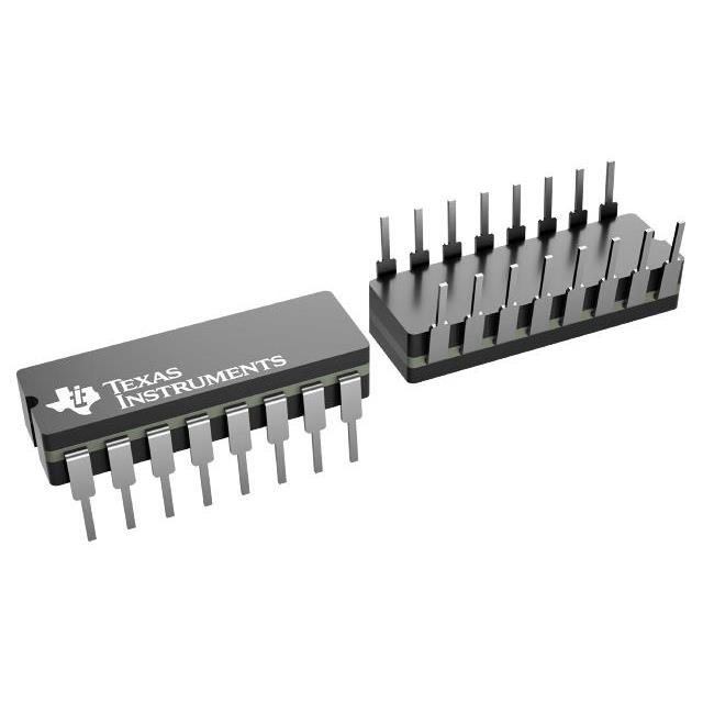
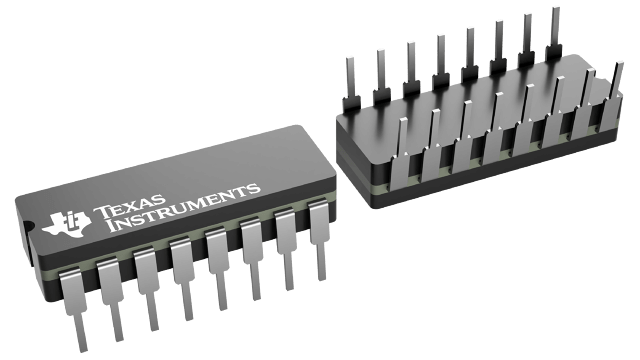
The CD4035B types are supplied in 16-lead hermetic dual-in-line ceramic packages (F3A suffix), 16-lead dual-in-line plastic packages (E suffix), 16-lead small-outline packages (M, M96, MT and NSR suffixes), and 16-lead thin shrink small-outline packages (PW and PWR suffixes).
CD4035B is a four-stage clocked signal serial register with provision for synchronous PARALLEL inputs to each stage and SERIAL inputs to the first stage via JK\ logic. Register stages 2, 3, and 4 are coupled in a serial D flip-flop configuration when the register is in the serial mode (PARALLEL/SERIAL control low).
Parallel entry into each register stage is permitted when the PARALLEL/SERIAL control is high.
In the parallel or serial mode information is transferred on positive clock transitions.
When the TRUE/COMPLEMENT control is high, the true contents of the register are available at the output terminals. When the TRUE/COMPLEMENT control is low, the outputs are the complements of the data in the register. THe TRUE/COMPLEMENT control functions asynchronously with respect to the CLOCK signal.
JK\ input logic is provided on the first stage SERIAL input to minimize logic requirements particularly in counting and sequence-generation applications. With JK\ inputs connected together, the first stage becomes a D flip-flop. An asynchronous common RESET is also provided.
The CD4035B types are supplied in 16-lead hermetic dual-in-line ceramic packages (F3A suffix), 16-lead dual-in-line plastic packages (E suffix), 16-lead small-outline packages (M, M96, MT and NSR suffixes), and 16-lead thin shrink small-outline packages (PW and PWR suffixes).