CD40109B-MIL Series
CMOS Quad Low-to-High Voltage Level Shifter (20V Rating)
Manufacturer: Texas Instruments
Catalog
CMOS Quad Low-to-High Voltage Level Shifter (20V Rating)
Description
AI
CD40109B contains four low-to-high-voltage level-shifting circuits. Each circuit will shift a low-voltage digital-logic input signal (A, B, C, D) with logical 1 = VCCand logical 0 = VSSto a higher-voltage output signal (E, F, G, H) with logical 1 = VDDand logical 0 = VSS.
The CD40109, unlike other low-to-high level-shifting circuits, does not require the presence of the high-voltage supply (VDD) before the application of either the low-voltage supply (VCC) or the input signals. There are no restrictions on the sequence of application of VDD, VCC, or the input signals. In addition, with one exception there are no restrictions on the relative magnitudes of the supply voltages or input signals within the device maximum ratings, provided that the input signal swings between VSSand at least 0.7 VCC; VCCmay exceed VDD, and input signals may exceed VCCand VDD. When operated in the mode VCC> VDD, the CD40109 will operate as a high-to-low level-shifter.
The CD40109 also features individual three-state output capability. A low level on any of the separately enabled three-state output controls produces a high-impedance state in the corresponding output.
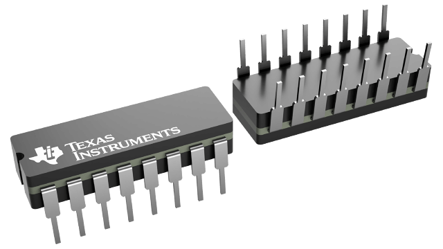
The CD40109B-Series types are supplied in 16-lead ceramic dual-in-line packages (F3A suffix), 16-lead dual-in-line plastic packages (E suffix), 16-lead small-outline packages (NSR suffix), and 16-lead thin shrink small-outline packages (PW and PWR suffixes).
CD40109B contains four low-to-high-voltage level-shifting circuits. Each circuit will shift a low-voltage digital-logic input signal (A, B, C, D) with logical 1 = VCCand logical 0 = VSSto a higher-voltage output signal (E, F, G, H) with logical 1 = VDDand logical 0 = VSS.
The CD40109, unlike other low-to-high level-shifting circuits, does not require the presence of the high-voltage supply (VDD) before the application of either the low-voltage supply (VCC) or the input signals. There are no restrictions on the sequence of application of VDD, VCC, or the input signals. In addition, with one exception there are no restrictions on the relative magnitudes of the supply voltages or input signals within the device maximum ratings, provided that the input signal swings between VSSand at least 0.7 VCC; VCCmay exceed VDD, and input signals may exceed VCCand VDD. When operated in the mode VCC> VDD, the CD40109 will operate as a high-to-low level-shifter.
The CD40109 also features individual three-state output capability. A low level on any of the separately enabled three-state output controls produces a high-impedance state in the corresponding output.
The CD40109B-Series types are supplied in 16-lead ceramic dual-in-line packages (F3A suffix), 16-lead dual-in-line plastic packages (E suffix), 16-lead small-outline packages (NSR suffix), and 16-lead thin shrink small-outline packages (PW and PWR suffixes).