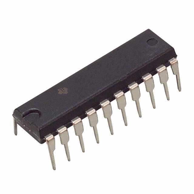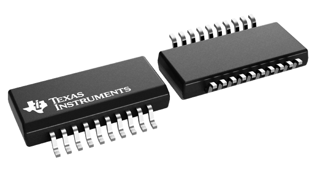
74FCT374 Series
BiCMOS FCT Interface Logic Octal D-Type Flip-Flops with 3-State Outputs
Manufacturer: Texas Instruments
Catalog
BiCMOS FCT Interface Logic Octal D-Type Flip-Flops with 3-State Outputs
Description
AI
The CD74FCT374 is an octal, edge-triggered, D-type flip-flop that uses a small-geometry BiCMOS technology and features 3-state outputs designed specifically for driving highly capacitive or relatively low-impedance loads. This device is particularly suitable for implementing buffer registers, I/O ports, bidirectional bus drivers, and working registers.
The output stage is a combination of bipolar and CMOS transistors that limits the output high level to two diode drops below VCC. This resultant lowering of output swing (0 V to 3.7 V) reduces power-bus ringing [a source of electromagnetic interference (EMI)] and minimizes VCCbounce and ground bounce and their effects during simultaneous output switching. The output configuration also enhances switching speed and is capable of sinking 48 mA.
The eight flip-flops enter data into their registers on the low-to-high transition of the clock (CLK). The output-enable (OE\) input controls the 3-state outputs and is independent of the register operation. When OE\ is high, the outputs are in the high-impedance state.
A buffered OE\ input can be used to place the eight outputs in either a normal logic state (high or low) or the high-impedance state. In the high-impedance state, the outputs neither load nor drive the bus lines significantly. The high-impedance state and the increased drive provide the capability to drive bus lines without interface or pullup components.
OE\ does not affect internal operations of the flip-flop. Old data can be retained or new data can be entered while the outputs are in the high-impedance state.
To ensure the high-impedance state during power up or power down, OE\ should be tied to VCCthrough a pullup resistor; the minimum value of the resistor is determined by the current-sinking capability of the driver.
The CD74FCT374 is characterized for operation from 0°C to 70°C.
The CD74FCT374 is an octal, edge-triggered, D-type flip-flop that uses a small-geometry BiCMOS technology and features 3-state outputs designed specifically for driving highly capacitive or relatively low-impedance loads. This device is particularly suitable for implementing buffer registers, I/O ports, bidirectional bus drivers, and working registers.
The output stage is a combination of bipolar and CMOS transistors that limits the output high level to two diode drops below VCC. This resultant lowering of output swing (0 V to 3.7 V) reduces power-bus ringing [a source of electromagnetic interference (EMI)] and minimizes VCCbounce and ground bounce and their effects during simultaneous output switching. The output configuration also enhances switching speed and is capable of sinking 48 mA.
The eight flip-flops enter data into their registers on the low-to-high transition of the clock (CLK). The output-enable (OE\) input controls the 3-state outputs and is independent of the register operation. When OE\ is high, the outputs are in the high-impedance state.
A buffered OE\ input can be used to place the eight outputs in either a normal logic state (high or low) or the high-impedance state. In the high-impedance state, the outputs neither load nor drive the bus lines significantly. The high-impedance state and the increased drive provide the capability to drive bus lines without interface or pullup components.
OE\ does not affect internal operations of the flip-flop. Old data can be retained or new data can be entered while the outputs are in the high-impedance state.
To ensure the high-impedance state during power up or power down, OE\ should be tied to VCCthrough a pullup resistor; the minimum value of the resistor is determined by the current-sinking capability of the driver.
The CD74FCT374 is characterized for operation from 0°C to 70°C.