MAX5530ETC+T
ActiveULTRA-LOW-POWER, 12-BIT, VOLTAGE-OUTPUT DACS
MAX5530ETC+T
ActiveULTRA-LOW-POWER, 12-BIT, VOLTAGE-OUTPUT DACS
Description
General part information
MAX5530 Series
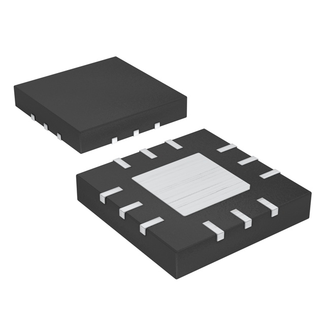
The MAX5530/MAX5531 are single, 12-bit, ultra-low- power, voltage-output, digital-to-analog converters (DACs) offering rail-to-rail buffered voltage outputs. The DACs operate from a 1.8V to 5.5V supply and consume less than 6µA, making them desirable for low-power and low-voltage applications. A shutdown mode reduces overall current, including the reference input current, to just 0.18µA. The MAX5530/MAX5531 use a 3-wire serial interface that is compatible with SPI™, QSPI™, and MICROWIRE™.At power-up, the MAX5530/MAX5531 outputs are driven to zero scale, providing additional safety for applications that drive valves or for other transducers that must be off during power-up. The zero-scale outputs enable glitch- free power-up.The MAX5530 accepts an external reference input. The MAX5531 contains an internal reference and provides an external reference output. Both devices have force-sense-configured output buffers.The MAX5530/MAX5531 are available in a 4mm x 4mm x 0.8mm, 12-pin, thin QFN package and are guaranteed over the extended -40°C to +85°C temperature range.For 10-bit compatible devices, refer to the MAX5520/MAX5521 data sheet. For 8-bit compatible devices, refer to the MAX5510/MAX5511 data sheet.ApplicationsAutomatic Trimming and Calibration in Factory or FieldChemical Sensor Cell Bias for Gas MonitorsIndustrial Process Control and Remote Industrial DevicesInstrumentationPortable Battery-Powered DevicesProgrammable Liquid Crystal Display (LCD) BiasProgrammable Voltage and Current SourcesRemote Data Conversion and Monitoring
Technical Specifications
Parameters and characteristics for this part
| Specification | MAX5530ETC+T |
|---|---|
| Architecture | R-2R |
| Data Interface | SPI |
| Differential Output | No |
| DNL (LSB) Tolerance | 0.2 LSB |
| INL (LSB) Tolerance | 4 LSB |
| Mounting Type | Surface Mount |
| Number of Bits | 12 bits |
| Number of D/A Converters | 1 count |
| Operating Temperature (Max) | 85 °C |
| Operating Temperature (Min) | -40 °C |
| Output Type | Voltage - Buffered |
| Package / Case | 12-WQFN Exposed Pad |
| Package Length | 4 mm |
| Package Name | 12-TQFN |
| Package Width | 4 mm |
| Reference Type | External |
| Settling Time (Typical) | 660 µs |
| Voltage - Supply, Analog (Max) | 5.5 V |
| Voltage - Supply, Analog (Min) | 1.8 V |
| Voltage - Supply, Digital (Max) | 5.5 V |
| Voltage - Supply, Digital (Min) | 1.8 V |
Pricing
Prices provided here are for design reference only. For realtime values and availability, please visit the distributors directly
Sign in to see pricing
Create a free account to access distributor pricing data.
CAD
3D models and CAD resources for this part
Documents
Technical documentation and resources