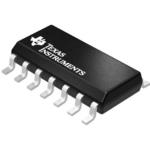
CD4011UBM
Obsolete4-CH, 2-INPUT, 3-V TO 18-V NAND GATES
CD4011UBM
Obsolete4-CH, 2-INPUT, 3-V TO 18-V NAND GATES
Description
General part information
CD4011 Series
CD4011UB quad 2-input NAND gate provides the system designer with direct implementation of the NAND function and supplements the existing family of CMOS gates.
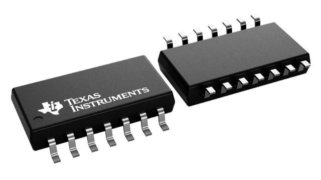
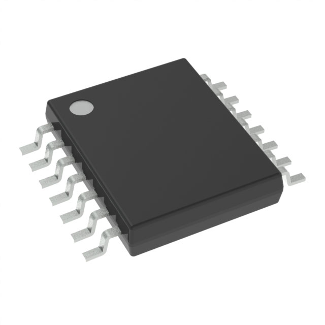
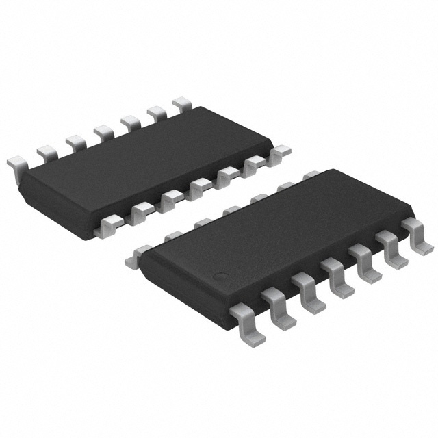
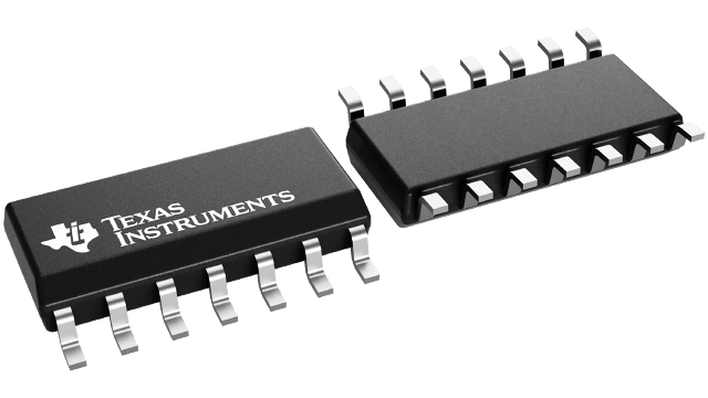
The CD4011UB types are supplied in 14-lead hermetic dual-in-line ceramic packages (F3A suffix), 14-lead dual-in-line plastic packages (E suffix), 14-lead small-outline package (M, MT, M96, NSR suffixes), and 14-lead thin shrink small-outline packages (PW and PWR suffixes).
CD4011UB quad 2-input NAND gate provides the system designer with direct implementation of the NAND function and supplements the existing family of CMOS gates.
Technical Specifications
Parameters and characteristics for this part
| Specification | CD4011UBM |
|---|---|
| Current - Output High | 3.4 mA |
| Current - Output Low | 3.4 mA |
| Current - Quiescent (Max) | 1 µA |
| Input Logic Level - High (Max) | 12.5 V |
| Input Logic Level - High (Min) | 4 V |
| Input Logic Level - Low (Max) | 2.5 V |
| Input Logic Level - Low (Min) | 1 V |
| Logic Type | NAND Gate |
| Max CL | 50 pF |
| Max Propagation Delay | 50 ns |
| Mounting Type | Surface Mount |
| Number of Circuits | 4 |
| Number of Inputs | 2 |
| Operating Temperature (Max) | 125 °C |
| Operating Temperature (Min) | -55 °C |
| Package Length | 0.154 in |
| Package Name | 14-SOIC |
| Package Width | 3.9 mm |
| Voltage - Supply (Maximum) | 18 V |
| Voltage - Supply (Minimum) | 3 V |
Pricing
Prices provided here are for design reference only. For realtime values and availability, please visit the distributors directly
Sign in to see pricing
Create a free account to access distributor pricing data.
CAD
3D models and CAD resources for this part
Documents
Technical documentation and resources