5962-8780601RA
ActiveHIGH SPEED CMOS LOGIC 8-BIT UNIVERSAL SHIFT REGISTER WITH 3-STATE OUTPUTS
Deep-Dive with AI
Search across all available documentation for this part.
5962-8780601RA
ActiveHIGH SPEED CMOS LOGIC 8-BIT UNIVERSAL SHIFT REGISTER WITH 3-STATE OUTPUTS
Technical Specifications
Parameters and characteristics commom to parts in this series
| Specification | 5962-8780601RA | CD54HC299 Series |
|---|---|---|
| Function | - | Universal |
| Logic Type | - | Shift Register |
| Mounting Type | - | Through Hole |
| null | - | |
| Number of Bits per Element | - | 8 |
| Number of Elements | - | 1 |
| Operating Temperature | - | -55 C |
| Operating Temperature | - | 125 °C |
| Output Type | - | Tri-State |
| Package / Case | - | 7.62 mm |
| Package / Case | - | 0.3 in |
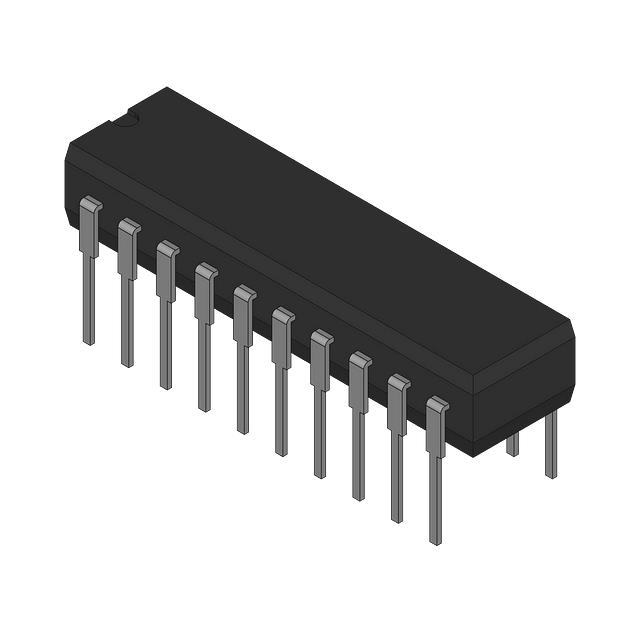
| Package / Case | - | 20-CDIP |
| Supplier Device Package | - | 20-CDIP |
| Voltage - Supply | - | 2 V |
| Voltage - Supply | - | 6 V |
Pricing
Prices provided here are for design reference only. For realtime values and availability, please visit the distributors directly
CD54HC299 Series
High Speed CMOS Logic 8-Bit Universal Shift Register with 3-State Outputs
| Part | Supplier Device Package | Output Type | Voltage - Supply [Min] | Voltage - Supply [Max] | Operating Temperature [Min] | Operating Temperature [Max] | Mounting Type | Logic Type | Function | Number of Bits per Element | Number of Elements [custom] | Package / Case | Package / Case | Package / Case |
|---|---|---|---|---|---|---|---|---|---|---|---|---|---|---|
Texas Instruments 5962-8780601RAThe ’HC259 and ’HCT299 are 8-bit shift/storage registers with three-state bus interface capability. The register has four synchronous-operating modes controlled by the two select inputs as shown in the mode select (S0, S1) table. The mode select, the serial data (DS0, DS7) and the parallel data (I/O0– I/O7) respond only to the low-to-high transition of the clock (CP) pulse. S0, S1 and data inputs must be one set-up time prior to the clock positive transition.
The Master Reset (MR)\ is an asynchronous active low input. When MR\ output is low, the register is cleared regardless of the status of all other inputs. The register can be expanded by cascading same units by tying the serial output (Q0) to the serial data (DS7) input of the preceding register, and tying the serial output (Q7) to the serial data (DS0) input of the following register. Recirculating the (n x 8) bits is accomplished by tying the Q7 of the last stage to the DS0 of the first stage.
The three-state input/output I(/O) port has three modes of operation:
1. Both output enable (OE1\ and OE2\) inputs are low and S0 or S1 or both are low, the data in the register is presented at the eight outputs.
2. When both S0 and S1 are high, I/O terminals are in the high impedance state but being input ports, ready for par-allel data to be loaded into eight registers with one clock transition regardless of the status of OE1\ and OE2\.
3. Either one of the two output enable inputs being high will force I/O terminals to be in the off-state. It is noted that each I/O terminal is a three-state output and a CMOS buffer input.
The ’HC259 and ’HCT299 are 8-bit shift/storage registers with three-state bus interface capability. The register has four synchronous-operating modes controlled by the two select inputs as shown in the mode select (S0, S1) table. The mode select, the serial data (DS0, DS7) and the parallel data (I/O0– I/O7) respond only to the low-to-high transition of the clock (CP) pulse. S0, S1 and data inputs must be one set-up time prior to the clock positive transition.
The Master Reset (MR)\ is an asynchronous active low input. When MR\ output is low, the register is cleared regardless of the status of all other inputs. The register can be expanded by cascading same units by tying the serial output (Q0) to the serial data (DS7) input of the preceding register, and tying the serial output (Q7) to the serial data (DS0) input of the following register. Recirculating the (n x 8) bits is accomplished by tying the Q7 of the last stage to the DS0 of the first stage.
The three-state input/output I(/O) port has three modes of operation:
1. Both output enable (OE1\ and OE2\) inputs are low and S0 or S1 or both are low, the data in the register is presented at the eight outputs.
2. When both S0 and S1 are high, I/O terminals are in the high impedance state but being input ports, ready for par-allel data to be loaded into eight registers with one clock transition regardless of the status of OE1\ and OE2\.
3. Either one of the two output enable inputs being high will force I/O terminals to be in the off-state. It is noted that each I/O terminal is a three-state output and a CMOS buffer input. | ||||||||||||||
Texas Instruments CD54HC299F3AThe ’HC259 and ’HCT299 are 8-bit shift/storage registers with three-state bus interface capability. The register has four synchronous-operating modes controlled by the two select inputs as shown in the mode select (S0, S1) table. The mode select, the serial data (DS0, DS7) and the parallel data (I/O0– I/O7) respond only to the low-to-high transition of the clock (CP) pulse. S0, S1 and data inputs must be one set-up time prior to the clock positive transition.
The Master Reset (MR)\ is an asynchronous active low input. When MR\ output is low, the register is cleared regardless of the status of all other inputs. The register can be expanded by cascading same units by tying the serial output (Q0) to the serial data (DS7) input of the preceding register, and tying the serial output (Q7) to the serial data (DS0) input of the following register. Recirculating the (n x 8) bits is accomplished by tying the Q7 of the last stage to the DS0 of the first stage.
The three-state input/output I(/O) port has three modes of operation:
1. Both output enable (OE1\ and OE2\) inputs are low and S0 or S1 or both are low, the data in the register is presented at the eight outputs.
2. When both S0 and S1 are high, I/O terminals are in the high impedance state but being input ports, ready for par-allel data to be loaded into eight registers with one clock transition regardless of the status of OE1\ and OE2\.
3. Either one of the two output enable inputs being high will force I/O terminals to be in the off-state. It is noted that each I/O terminal is a three-state output and a CMOS buffer input.
The ’HC259 and ’HCT299 are 8-bit shift/storage registers with three-state bus interface capability. The register has four synchronous-operating modes controlled by the two select inputs as shown in the mode select (S0, S1) table. The mode select, the serial data (DS0, DS7) and the parallel data (I/O0– I/O7) respond only to the low-to-high transition of the clock (CP) pulse. S0, S1 and data inputs must be one set-up time prior to the clock positive transition.
The Master Reset (MR)\ is an asynchronous active low input. When MR\ output is low, the register is cleared regardless of the status of all other inputs. The register can be expanded by cascading same units by tying the serial output (Q0) to the serial data (DS7) input of the preceding register, and tying the serial output (Q7) to the serial data (DS0) input of the following register. Recirculating the (n x 8) bits is accomplished by tying the Q7 of the last stage to the DS0 of the first stage.
The three-state input/output I(/O) port has three modes of operation:
1. Both output enable (OE1\ and OE2\) inputs are low and S0 or S1 or both are low, the data in the register is presented at the eight outputs.
2. When both S0 and S1 are high, I/O terminals are in the high impedance state but being input ports, ready for par-allel data to be loaded into eight registers with one clock transition regardless of the status of OE1\ and OE2\.
3. Either one of the two output enable inputs being high will force I/O terminals to be in the off-state. It is noted that each I/O terminal is a three-state output and a CMOS buffer input. | 20-CDIP | Tri-State | 2 V | 6 V | -55 C | 125 °C | Through Hole | Shift Register | Universal | 8 | 1 | 7.62 mm | 0.3 in | 20-CDIP |
Description
General part information
CD54HC299 Series
The ’HC259 and ’HCT299 are 8-bit shift/storage registers with three-state bus interface capability. The register has four synchronous-operating modes controlled by the two select inputs as shown in the mode select (S0, S1) table. The mode select, the serial data (DS0, DS7) and the parallel data (I/O0– I/O7) respond only to the low-to-high transition of the clock (CP) pulse. S0, S1 and data inputs must be one set-up time prior to the clock positive transition.
The Master Reset (MR)\ is an asynchronous active low input. When MR\ output is low, the register is cleared regardless of the status of all other inputs. The register can be expanded by cascading same units by tying the serial output (Q0) to the serial data (DS7) input of the preceding register, and tying the serial output (Q7) to the serial data (DS0) input of the following register. Recirculating the (n x 8) bits is accomplished by tying the Q7 of the last stage to the DS0 of the first stage.
The three-state input/output I(/O) port has three modes of operation:
Documents
Technical documentation and resources