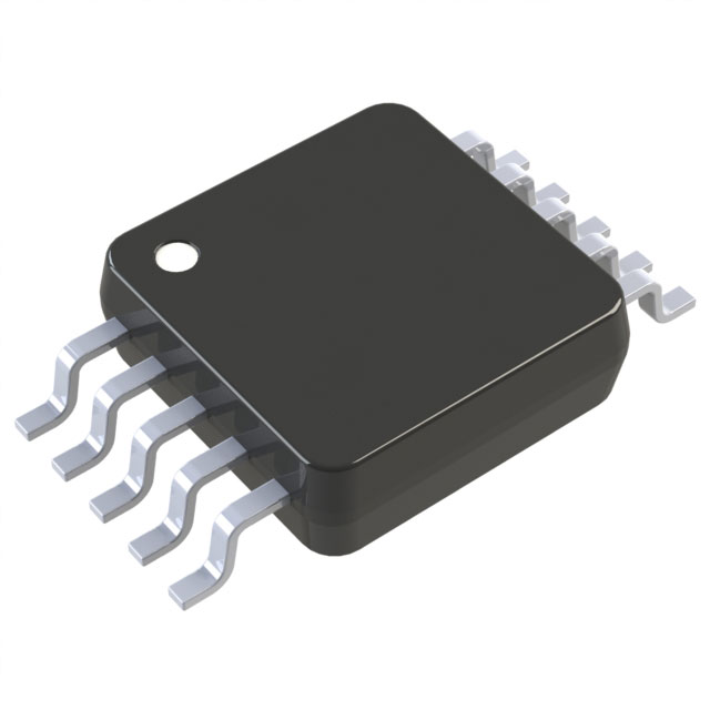
LTC2642CMS-14#PBF
Active16-/14-/12-BIT VOUTDACS IN 3MM × 3MM DFN
Deep-Dive with AI
Search across all available documentation for this part.

LTC2642CMS-14#PBF
Active16-/14-/12-BIT VOUTDACS IN 3MM × 3MM DFN
Deep-Dive with AI
Technical Specifications
Parameters and characteristics for this part
| Specification | LTC2642CMS-14#PBF |
|---|---|
| Architecture | R-2R |
| Data Interface | SPI |
| Differential Output | False |
| INL/DNL (LSB) | 0.5 LSB |
| Mounting Type | Surface Mount |
| Number of Bits | 14 |
| Operating Temperature [Max] | 70 °C |
| Operating Temperature [Min] | 0 °C |
| Output Type | Voltage - Unbuffered |
| Package / Case | 10-MSOP, 10-TFSOP |
| Package / Case [x] | 3 mm |
| Package / Case [x] | 0.118 in |
| Reference Type | External |
| Settling Time | 1 µs |
| Supplier Device Package | 10-MSOP |
| Voltage - Supply, Analog [Max] | 5.5 V |
| Voltage - Supply, Analog [Min] | 2.7 V |
| Voltage - Supply, Digital [Max] | 5.5 V |
| Voltage - Supply, Digital [Min] | 2.7 V |
Pricing
Prices provided here are for design reference only. For realtime values and availability, please visit the distributors directly
| Distributor | Package | Quantity | $ | |
|---|---|---|---|---|
| Digikey | Tube | 50 | $ 9.77 | |
Description
General part information
LTC2642 Series
The LTC2641/LTC2642 are families of 16-, 14- and 12-bit unbuffered voltage output DACs. These DACs operate from a single 2.7V to 5.5V supply and are guaranteed monotonic over temperature. The LTC2641A-16/LTC2642A-16 provide 16-bit performance (±1LSB INL and ±1LSB DNL) over temperature. Unbuffered DAC outputs result in low supply current of 120µA and a low offset error of ±1LSB.Both the LTC2641 and LTC2642 feature a reference input range of 2V to VDD. VOUTswings from 0V to VREF. For bipolar operation, the LTC2642 includes matched scaling resistors for use with an external precision op amp (such as the LT1678), generating a ±VREFoutput swing at RFB.The LTC2641/LTC2642 use a simple SPI/MICROWIRE compatible 3-wire serial interface which can be operated at clock rates up to 50MHz and can interface directly with optocouplers for applications requiring isolation. A power-on reset circuit clears the LTC2641’s DAC output to zero scale and the LTC2642’s DAC output to midscale when power is initially applied. A logic low on theCLRpin asynchronously clears the DAC to zero scale (LTC2641) or midscale (LTC2642). These DACs are all specified over the commercial and industrial ranges.ApplicationsHigh Resolution Offset and Gain AdjustmentProcess Control and Industrial AutomationAutomatic Test EquipmentData Aquisition Systems
Documents
Technical documentation and resources


