854110AYILFT
Obsolete2.5V DIFFERENTIAL LVDS CLOCK BUFFER
854110AYILFT
Obsolete2.5V DIFFERENTIAL LVDS CLOCK BUFFER
Description
General part information
854110I Series
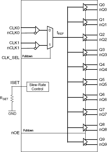
The 854110I is a high-performance differential LVDS clock fanout buffer. The device is designed for signal fanout of high-frequency, low phase-noise clock signals. The selected differential input signal is distributed to ten differential LVDS outputs. The 854110I is characterized to operate from a 2.5V power supply. Guaranteed output-to-output and part-to-part skew characteristics make the 854110I ideal for those clock distribution applications demanding well-defined performance and repeatability. The device offers an output slew rate control with four pre-set output transition times to solve crosstalk and EMI problems in complex board designs. A fail-safe input design forces the outputs to a defined state if differential clock inputs are open or shorted, see Table 3D.
Technical Specifications
Parameters and characteristics for this part
| Specification | 854110AYILFT |
|---|---|
| Differential Input | Yes |
| Differential Output | Yes |
| Frequency - Max | 16 MHz |
| Input | LVDS, LVPECL |
| Input Ratio | 2 |
| Mounting Type | Surface Mount |
| Number of Circuits | 1 |
| Operating Temperature (Max) | 85 °C |
| Operating Temperature (Min) | -40 °C |
| Output | LVDS |
| Output Ratio | 10 |
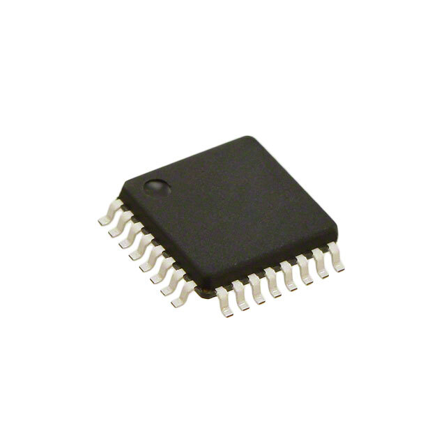
| Package / Case | 32-LQFP |
| Package Length | 7 mm |
| Package Name | 32-TQFP |
| Package Width | 7 mm |
| Type | Multiplexer, Fanout Buffer (Distribution) |
| Voltage - Supply (Maximum) | 2.625 V |
| Voltage - Supply (Minimum) | 2.375 V |
Pricing
Prices provided here are for design reference only. For realtime values and availability, please visit the distributors directly
Sign in to see pricing
Create a free account to access distributor pricing data.
CAD
3D models and CAD resources for this part
Documents
Technical documentation and resources