


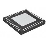
MAX2067ETL+T
Active50MHZ TO 1000MHZ HIGH-LINEARITY, SERIAL/ANALOG-CONTROLLED VGA

MAX2067ETL+T
Active50MHZ TO 1000MHZ HIGH-LINEARITY, SERIAL/ANALOG-CONTROLLED VGA
Description
General part information
MAX2067 Series
The MAX2067 high-linearity analog variable-gain amplifier (VGA) is a monolithic SiGe BiCMOS attenuator and amplifier designed to interface with 50Ω systems operating in the 50MHz to 1000MHz frequency range (see theTypical Application Circuitin the full data sheet). The analog attenuator is controlled using an external voltage or through the SPI™-compatible interface using an on-chip 8-bit DAC.Because each stage has its own RF input and RF output, this component can be configured to either optimize NF (amplifier configured first), or OIP3 (amplifier last). The device's performance features include 22dB amplifier gain (amplifier only), 4dB NF at maximum gain (includes attenuator insertion loss), and a high OIP3 level of +43dBm. Each of these features makes the MAX2067 an ideal VGA for numerous receiver and transmitter applications.In addition, the MAX2067 operates from a single +5V supply with full performance, or a single +3.3V supply with slightly reduced performance, and has an adjustable bias to trade current consumption for linearity performance. This device is available in a compact 40-pin thin QFN package (6mm x 6mm) with an exposed pad. Electrical performance is guaranteed over the extended temperature range (TC= -40°C to +85°C).ApplicationsCable Modem Termination Systems (CMTS)Cellular Band WCDMA and cdma2000® Base StationsFixed Broadband Wireless AccessGSM 850/GSM 900 EDGE Base StationsIF and RF Gain StagesMilitary SystemsRFID Handheld and Portal ReadersTemperature Compensation CircuitsVideo-on-Demand (VOD) and DOCSIS®-Compliant EDGE QAM ModulationWiMAX and LTE Base Stations and Customer Premise EquipmentWireless Local Loop
Technical Specifications
Parameters and characteristics for this part
| Specification | MAX2067ETL+T |
|---|---|
| Current - Supply | 123 mA |
| Frequency (Max) | 1 GHz |
| Frequency (Min) | 50 MHz |
| Gain | 21.3 dB |
| Mounting Type | Surface Mount |
| Noise Figure | 4.2 dB |
| P1dB | 18.7 dBm |
| Package / Case | 40-WFQFN Exposed Pad |
| Package Length | 6 mm |
| Package Name | 40-TQFN |
| Package Width | 6 mm |
| RF Type | CDMA, Cellular, GSM |
| Test Frequency | 350 MHz |
| Voltage - Supply (Range 1 Maximum) | 3.6 V |
| Voltage - Supply (Range 1 Minimum) | 3 V |
| Voltage - Supply (Range 2 Maximum) | 5.25 V |
| Voltage - Supply (Range 2 Minimum) | 4.75 V |
Pricing
Prices provided here are for design reference only. For realtime values and availability, please visit the distributors directly
Sign in to see pricing
Create a free account to access distributor pricing data.
CAD
3D models and CAD resources for this part
Documents
Technical documentation and resources