STM32F777IIK7
ActiveHIGH-PERFORMANCE AND DSP WITH FPU, ARM CORTEX-M7 MCU WITH 2 MBYTES OF FLASH MEMORY, 216 MHZ CPU, ART ACCELERATOR, L1 CACHE, HW CRYPTO, SDRAM, TFT, JPEG CODEC, DFSDM
Technical Specifications
Parameters and characteristics for this part
| Specification | STM32F777IIK7 |
|---|---|
| Connectivity | QSPI, MMC/SD/SDIO, SAI, EBI/EMI, CANbus, SPDIF, I2C, Ethernet, USB OTG, SPI, UART/USART, LINbus, IrDA |
| Core Processor | ARM® Cortex®-M7 |
| Core Size | 32-Bit Single-Core |
| Data Converters | A/D 24x12b, D/A 2x12b |
| Mounting Type | Surface Mount |
| Number of I/O | 132 |
| Operating Temperature [Max] | 105 °C |
| Operating Temperature [Min] | -40 °C |
| Oscillator Type | Internal |
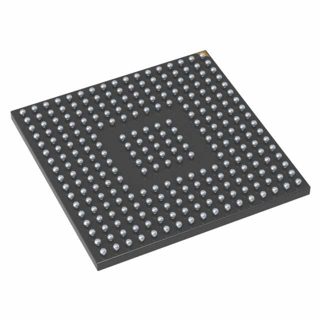
| Package / Case | 201-UFBGA |
| Peripherals | WDT, I2S, Brown-out Detect/Reset, POR, PWM, LCD, DMA |
| Program Memory Size | 2 MB |
| Program Memory Type | FLASH |
| RAM Size | 512 K |
| Speed | 216 MHz |
| Supplier Device Package | 176+25UFBGA (10x10) |
| Voltage - Supply (Vcc/Vdd) [Max] | 3.6 V |
| Voltage - Supply (Vcc/Vdd) [Min] | 1.7 V |
Pricing
Prices provided here are for design reference only. For realtime values and availability, please visit the distributors directly
Description
General part information
STM32F777II Series
The STM32F777xx, STM32F778Ax and STM32F779xx devices are based on the high-performance Arm®Cortex®-M7 32-bit RISC core operating at up to 216 MHz frequency. The Cortex®-M7 core features a floating point unit (FPU), which supports Arm®double-precision and single-precision data-processing instructions and data types. It also implements a full set of DSP instructions and a memory protection unit (MPU), which enhances the application security.
The STM32F777xx, STM32F778Ax and STM32F779xx devices incorporate high-speed embedded memories with a flash up to 2 Mbytes, 512 Kbytes of SRAM (including 128 Kbytes of Data TCM RAM for critical real-time data), 16 Kbytes of instruction TCM RAM (for critical real-time routines), 4 Kbytes of backup SRAM available in the lowest power modes, and an extensive range of enhanced I/Os and peripherals connected to two APB buses, two AHB buses, a 32-bit multi-AHB bus matrix, and a multi layer AXI interconnect supporting internal and external memories access.
The devices offer three 12-bit ADCs, two DACs, a low-power RTC, twelve general-purpose 16-bit timers including two PWM timers for motor control, two general-purpose 32-bit timers, a true random number generator (RNG), and a cryptographic acceleration cell. They also feature standard and advanced communication interfaces.
Documents
Technical documentation and resources