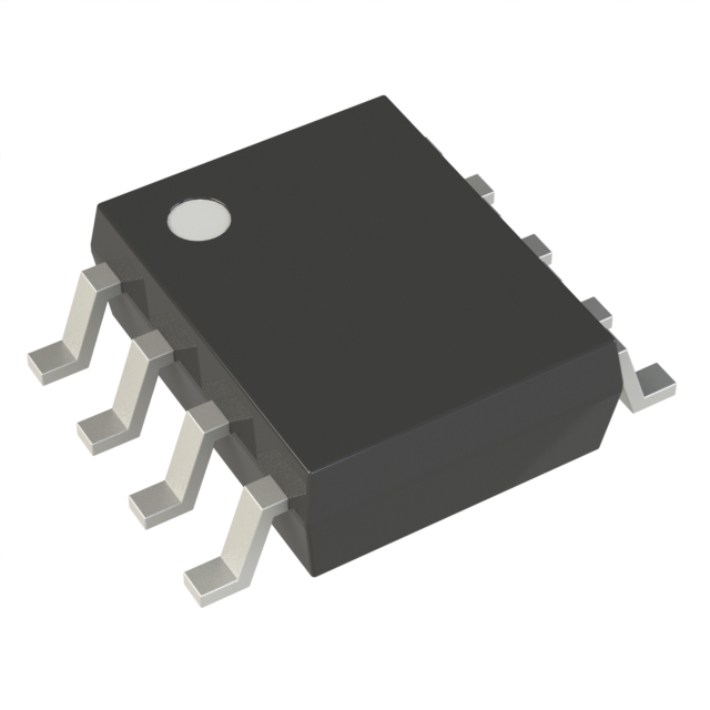
M24256-BRMN6TP
ActiveEEPROM SERIAL-I2C 256K-BIT 32K X 8 2.5V/3.3V/5V 8-PIN SO N T/R
Deep-Dive with AI
Search across all available documentation for this part.

M24256-BRMN6TP
ActiveEEPROM SERIAL-I2C 256K-BIT 32K X 8 2.5V/3.3V/5V 8-PIN SO N T/R
Deep-Dive with AI
Technical Specifications
Parameters and characteristics for this part
| Specification | M24256-BRMN6TP |
|---|---|
| Access Time | 450 ns |
| Memory Format | EEPROM |
| Memory Interface | I2C |
| Memory Organization | 32K x 8 |
| Memory Size | 32 KB |
| Memory Type | Non-Volatile |
| Mounting Type | Surface Mount |
| Operating Temperature [Max] | 85 °C |
| Operating Temperature [Min] | -40 °C |
| Package / Case | 8-SOIC |
| Package / Case [x] | 0.154 in |
| Package / Case [y] | 3.9 mm |
| Supplier Device Package | 8-SOIC |
| Technology | EEPROM |
| Voltage - Supply [Max] | 5.5 V |
| Voltage - Supply [Min] | 1.8 V |
| Write Cycle Time - Word, Page | 5 ms |
Pricing
Prices provided here are for design reference only. For realtime values and availability, please visit the distributors directly
| Distributor | Package | Quantity | $ | |
|---|---|---|---|---|
| Digikey | Cut Tape (CT) | 1 | $ 0.41 | |
| 10 | $ 0.41 | |||
| 25 | $ 0.38 | |||
| 50 | $ 0.38 | |||
| 100 | $ 0.33 | |||
| 250 | $ 0.33 | |||
| 500 | $ 0.32 | |||
| 1000 | $ 0.32 | |||
| Digi-Reel® | 1 | $ 0.41 | ||
| 10 | $ 0.41 | |||
| 25 | $ 0.38 | |||
| 50 | $ 0.38 | |||
| 100 | $ 0.33 | |||
| 250 | $ 0.33 | |||
| 500 | $ 0.32 | |||
| 1000 | $ 0.32 | |||
| Tape & Reel (TR) | 2500 | $ 0.31 | ||
| 5000 | $ 0.28 | |||
| 12500 | $ 0.28 | |||
| 25000 | $ 0.27 | |||
| Newark | Each (Supplied on Full Reel) | 2500 | $ 0.39 | |
| 5000 | $ 0.38 | |||
| 10000 | $ 0.38 | |||
| 15000 | $ 0.38 | |||
| 25000 | $ 0.37 | |||
Description
General part information
M24256-A125 Series
The M24256X-F is a 256-Kbit I2C-compatible EEPROM (electrically erasable programmable memory) organized as 32 K × 8 bits.
The M24256X-F can operate with a supply voltage from 1.65 V to 3.6 V, with a clock frequency up to 1 MHz, over an ambient temperature range from -40 °C to +85 °C. It can also operate down to 1.6 V, under some restricting conditions.
The M24256X-F offers three additional features, namely a 64-byte page, named identification page, which can be used to store sensitive application parameters that can be (later) permanently locked in read-only mode, a first 8-bit register, named configurable device address (CDA) register, authorizing the user, through software, to configure up to eight possibilities of chip enable address, and a second 8-bit register, named software write protection (SWP) register, authorizing the user, through software, to write protect a part or the full memory array.
Documents
Technical documentation and resources


