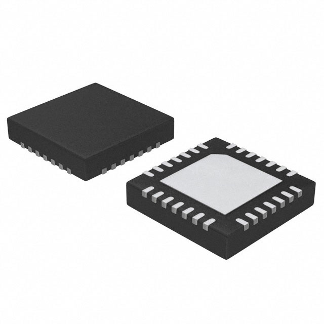
MAX11128ATI/V+T
Active1MSPS, LOW-POWER, SERIAL 12-/10-/8-BIT, 4-/8-/16-CHANNEL ADCS
MAX11128ATI/V+T
Active1MSPS, LOW-POWER, SERIAL 12-/10-/8-BIT, 4-/8-/16-CHANNEL ADCS
Description
General part information
MAX11128 Series
The MAX11120–MAX11128 are 12-/10-/8-bit with external reference and industry-leading 1.5MHz, full linear bandwidth, high speed, low-power, serial output successive approximation register (SAR) analog-to-digital converters (ADCs). The MAX11120–MAX11128 include both internal and external clock modes. These devices feature scan mode in both internal and external clock modes. The internal clock mode features internal averaging to increase SNR. The external clock mode features the SampleSet™ technology, a user-programmable analog input channel sequencer. The SampleSet approach provides greater sequencing flexibility for multichannel applications while alleviating significant microcontroller or DSP (controlling unit) communication overhead.The internal clock mode features an integrated FIFO allowing data to be sampled at high speeds and then held for readout at any time or at a lower clock rate. Internal averaging is also supported in this mode improving SNR for noisy input signals. The devices feature analog input channels that can be configured to be single-ended inputs, fully differential pairs, or pseudo-differential inputs with respect to one common input. The MAX11120–MAX11128 operate from a 2.35V to 3.6V supply and consume only 5.4mW at 1Msps.The MAX11120–MAX11128 include AutoShutdown™, fast wake-up, and a high-speed 3-wire serial interface. The devices feature full power-down mode for optimal power management.The 16MHz, 3-wire serial interface directly connects to SPI, QSPI™, and MICROWIRE®devices without external logic.Excellent dynamic performance, low voltage, low power, ease of use, and small package size make these converters ideal for portable battery-powered data-acquisition applications, and for other applications that demand low power consumption and small space.The MAX11120–MAX11128 are available in 28-pin, 5mm x 5mm, TQFN packages and operate over the -40°C to +125°C temperature range.ApplicationsBattery-Powered InstrumentsHigh-Speed Closed-Loop SystemsHigh-Speed Data Acquisition SystemsIndustrial Control SystemsMedical InstrumentationPortable Systems
Technical Specifications
Parameters and characteristics for this part
| Specification | MAX11128ATI/V+T |
|---|---|
| Architecture | SAR |
| Configuration | MUX-S/H-ADC |
| Data Interface | SPI |
| Input Type | Single Ended, Pseudo-Differential, Differential |
| Mounting Type | Surface Mount |
| Number of A/D Converters | 1 count |
| Number of Bits | 12 bits |
| Number of Inputs | 16 |
| Operating Temperature (Max) | 125 °C |
| Operating Temperature (Min) | -40 °C |
| Package / Case | 28-WFQFN Exposed Pad |
| Package Length | 5 mm |
| Package Name | 28-TQFN |
| Package Width | 5 mm |
| Ratio - ADC | 1 |
| Ratio - S/H | 1 |
| Reference Type | External |
| Sampling Rate (Per Second) | 1 MHz |
| Voltage - Supply, Analog (Max) | 3.6 V |
| Voltage - Supply, Analog (Min) | 2.35 V |
| Voltage - Supply, Digital (Max) | 3.6 V |
| Voltage - Supply, Digital (Min) | 1.5 V |
Pricing
Prices provided here are for design reference only. For realtime values and availability, please visit the distributors directly
Sign in to see pricing
Create a free account to access distributor pricing data.
CAD
3D models and CAD resources for this part
Documents
Technical documentation and resources