TPD2S017DBVR
Active2 CHANNEL 5.5-V, 1-PF, ±11KV ESD PROTECTION DIODE WITH LOW CLAMPING AND EMI FILTERING 6-SOT-23 -40 TO 85
Deep-Dive with AI
Search across all available documentation for this part.
TPD2S017DBVR
Active2 CHANNEL 5.5-V, 1-PF, ±11KV ESD PROTECTION DIODE WITH LOW CLAMPING AND EMI FILTERING 6-SOT-23 -40 TO 85
Technical Specifications
Parameters and characteristics for this part
| Specification | TPD2S017DBVR |
|---|---|
| Applications | General Purpose |
| Mounting Type | Surface Mount |
| Number of Circuits | 2 |
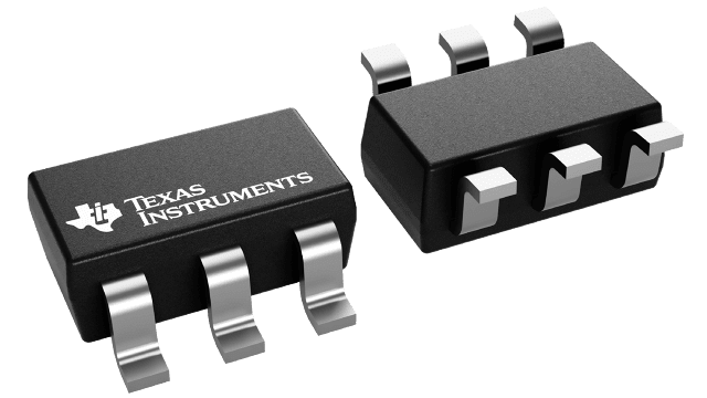
| Package / Case | SOT-23-6 |
| Supplier Device Package | SOT-23-6 |
| Technology | Mixed Technology |
| Voltage - Clamping | 11 V |
Pricing
Prices provided here are for design reference only. For realtime values and availability, please visit the distributors directly
TPD2S017 Series
2 channel 5.5-V, 1-pF, ±11kV ESD protection diode with low clamping and EMI filtering
| Part | Voltage - Clamping | Technology | Number of Circuits | Supplier Device Package | Applications | Mounting Type | Package / Case |
|---|---|---|---|---|---|---|---|
Texas Instruments TPD2S017DBVRThe TPD2S017 is a two channel electrostatic discharge (ESD) protection device. This protection product offers two-stage ESD transient voltage suppression (TVS) diodes in each line with a typically 1-Ω series resistor isolation. This architecture allows the device to clamp at a very low voltage during system level ESD strikes.
The TPD2S017 conforms to the IEC61000-4-2 ESD protection standard. Due to the series resistor component, the TPD2S017 provides a controlled filter roll-off for even greater spurious EMI suppression and signal integrity. The monolithic silicon technology allows good matching of the component values, including the clamp capacitances and the series resistors between the differential signal pairs. The tight matching of the line capacitance and series resistors ensures that the differential signal distortion due to added ESD clamp remains minimal, and it also allows the part to operate at high-speed differential data rate (in excess of 1.5 Gbps). The DBV package offers a flow-through pin mapping for ease of board layout.
Typical applications of this ESD protection device are circuit protection for USB data lines, IEEE 1394 Interfaces, LVDS, MDDI/MIPI and HS signals.
The TPD2S017 is a two channel electrostatic discharge (ESD) protection device. This protection product offers two-stage ESD transient voltage suppression (TVS) diodes in each line with a typically 1-Ω series resistor isolation. This architecture allows the device to clamp at a very low voltage during system level ESD strikes.
The TPD2S017 conforms to the IEC61000-4-2 ESD protection standard. Due to the series resistor component, the TPD2S017 provides a controlled filter roll-off for even greater spurious EMI suppression and signal integrity. The monolithic silicon technology allows good matching of the component values, including the clamp capacitances and the series resistors between the differential signal pairs. The tight matching of the line capacitance and series resistors ensures that the differential signal distortion due to added ESD clamp remains minimal, and it also allows the part to operate at high-speed differential data rate (in excess of 1.5 Gbps). The DBV package offers a flow-through pin mapping for ease of board layout.
Typical applications of this ESD protection device are circuit protection for USB data lines, IEEE 1394 Interfaces, LVDS, MDDI/MIPI and HS signals. | 11 V | Mixed Technology | 2 | SOT-23-6 | General Purpose | Surface Mount | SOT-23-6 |
Description
General part information
TPD2S017 Series
The TPD2S017 is a two channel electrostatic discharge (ESD) protection device. This protection product offers two-stage ESD transient voltage suppression (TVS) diodes in each line with a typically 1-Ω series resistor isolation. This architecture allows the device to clamp at a very low voltage during system level ESD strikes.
The TPD2S017 conforms to the IEC61000-4-2 ESD protection standard. Due to the series resistor component, the TPD2S017 provides a controlled filter roll-off for even greater spurious EMI suppression and signal integrity. The monolithic silicon technology allows good matching of the component values, including the clamp capacitances and the series resistors between the differential signal pairs. The tight matching of the line capacitance and series resistors ensures that the differential signal distortion due to added ESD clamp remains minimal, and it also allows the part to operate at high-speed differential data rate (in excess of 1.5 Gbps). The DBV package offers a flow-through pin mapping for ease of board layout.
Typical applications of this ESD protection device are circuit protection for USB data lines, IEEE 1394 Interfaces, LVDS, MDDI/MIPI and HS signals.
Documents
Technical documentation and resources