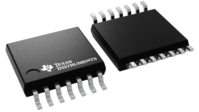
SN74LVC126APW
ActiveFOUR-CHANNEL, 1.65V TO 3.6V BUFFERS WITH THREE-STATE OUTPUTS
Deep-Dive with AI
Search across all available documentation for this part.
SN74LVC126APW
ActiveFOUR-CHANNEL, 1.65V TO 3.6V BUFFERS WITH THREE-STATE OUTPUTS
Technical Specifications
Parameters and characteristics commom to parts in this series
| Specification | SN74LVC126APW | 74LVC126 Series |
|---|---|---|
| Current - Output High, Low [custom] | 24 mA | 24 mA |
| Current - Output High, Low [custom] | 24 mA | 24 mA |
| Grade | - | Automotive |
| Logic Type | Buffer, Non-Inverting | Buffer, Non-Inverting |
| Mounting Type | Surface Mount | Surface Mount |
| Number of Bits per Element | 1 | 1 |
| Number of Elements | 4 | 4 |
| Operating Temperature [Max] | 125 °C | 85 - 125 °C |
| Operating Temperature [Min] | -40 °C | -40 °C |
| Output Type | 3-State | 3-State |
| Package / Case | 14-TSSOP | 14-TSSOP, 14-VFQFN Exposed Pad, 14-SOIC, 14-SSOP, 14-TFSOP |
| Package / Case | - | 3.9 mm |
| Package / Case | - | 0.154 - 5.3 in |
| Package / Case | - | 5.3 mm |
| Package / Case | - | 0.209 in |
| Package / Case | - | 0.209 - 4.4 in |
| Package / Case [custom] | 0.173 in | 0.173 in |
| Package / Case [custom] | 4.4 mm | 4.4 mm |
| Qualification | - | AEC-Q100 |
| Supplier Device Package | 14-TSSOP | 14-TSSOP, 14-VQFN (3.5x3.5), 14-SO, 14-SSOP |
| Voltage - Supply [Max] | 3.6 V | 3.6 V |
| Voltage - Supply [Min] | 1.65 V | 1.65 V |
Pricing
Prices provided here are for design reference only. For realtime values and availability, please visit the distributors directly
74LVC126 Series
Four-channel, 1.65V to 3.6V buffers with three-state outputs
| Part | Qualification | Mounting Type | Logic Type | Output Type | Number of Bits per Element | Supplier Device Package | Voltage - Supply [Max] | Voltage - Supply [Min] | Operating Temperature [Min] | Operating Temperature [Max] | Grade | Package / Case | Package / Case [custom] | Package / Case [custom] | Current - Output High, Low [custom] | Current - Output High, Low [custom] | Number of Elements | Package / Case | Package / Case | Package / Case [y] | Package / Case [y] | Package / Case |
|---|---|---|---|---|---|---|---|---|---|---|---|---|---|---|---|---|---|---|---|---|---|---|
Texas Instruments SN74LVC126AQPWRQ1Buffer, Non-Inverting 4 Element 1 Bit per Element 3-State Output 14-TSSOP | AEC-Q100 | Surface Mount | Buffer, Non-Inverting | 3-State | 1 | 14-TSSOP | 3.6 V | 1.65 V | -40 °C | 125 °C | Automotive | 14-TSSOP | 0.173 in | 4.4 mm | 24 mA | 24 mA | 4 | |||||
Texas Instruments SN74LVC126APWTBuffer, Non-Inverting 4 Element 1 Bit per Element 3-State Output 14-TSSOP | Surface Mount | Buffer, Non-Inverting | 3-State | 1 | 14-TSSOP | 3.6 V | 1.65 V | -40 °C | 125 °C | 14-TSSOP | 0.173 in | 4.4 mm | 24 mA | 24 mA | 4 | |||||||
Texas Instruments SN74LVC126ARGYRG4Buffer, Non-Inverting 4 Element 1 Bit per Element 3-State Output 14-VQFN (3.5x3.5) | Surface Mount | Buffer, Non-Inverting | 3-State | 1 | 14-VQFN (3.5x3.5) | 3.6 V | 1.65 V | -40 °C | 85 °C | 14-VFQFN Exposed Pad | 24 mA | 24 mA | 4 | |||||||||
Texas Instruments SN74LVC126ADG4Buffer, Non-Inverting 4 Element 1 Bit per Element 3-State Output 14-SOIC | Surface Mount | Buffer, Non-Inverting | 3-State | 1 | 3.6 V | 1.65 V | -40 °C | 125 °C | 14-SOIC | 24 mA | 24 mA | 4 | 3.9 mm | 0.154 in | ||||||||
Texas Instruments SN74LVC126ANSRThe SN74LVC126A device is a quadruple bus buffer gate designed for 1.65V to 3.6V VCC operation.
The SN74LVC126A device features independent line drivers with 3-state outputs. Each output is disabled when the associated output-enable (OE) input is low.
To ensure the high-impedance state during power up or power down, OE must be tied to GND through a pulldown resistor; the minimum value of the resistor is determined by the current-sourcing capability of the driver.
Inputs can be driven from either 3.3V or 5V devices. This feature allows the use of this device as a translator in a mixed 3.3V and 5V system environment.
The SN74LVC126A device is a quadruple bus buffer gate designed for 1.65V to 3.6V VCC operation.
The SN74LVC126A device features independent line drivers with 3-state outputs. Each output is disabled when the associated output-enable (OE) input is low.
To ensure the high-impedance state during power up or power down, OE must be tied to GND through a pulldown resistor; the minimum value of the resistor is determined by the current-sourcing capability of the driver.
Inputs can be driven from either 3.3V or 5V devices. This feature allows the use of this device as a translator in a mixed 3.3V and 5V system environment. | Surface Mount | Buffer, Non-Inverting | 3-State | 1 | 14-SO | 3.6 V | 1.65 V | -40 °C | 125 °C | 14-SOIC | 24 mA | 24 mA | 4 | 5.3 mm | 0.209 in | |||||||
Texas Instruments SN74LVC126ADRG4Buffer, Non-Inverting 4 Element 1 Bit per Element 3-State Output 14-SOIC | Surface Mount | Buffer, Non-Inverting | 3-State | 1 | 3.6 V | 1.65 V | -40 °C | 125 °C | 14-SOIC | 24 mA | 24 mA | 4 | 3.9 mm | 0.154 in | ||||||||
Texas Instruments SN74LVC126ADBRThe SN74LVC126A device is a quadruple bus buffer gate designed for 1.65V to 3.6V VCC operation.
The SN74LVC126A device features independent line drivers with 3-state outputs. Each output is disabled when the associated output-enable (OE) input is low.
To ensure the high-impedance state during power up or power down, OE must be tied to GND through a pulldown resistor; the minimum value of the resistor is determined by the current-sourcing capability of the driver.
Inputs can be driven from either 3.3V or 5V devices. This feature allows the use of this device as a translator in a mixed 3.3V and 5V system environment.
The SN74LVC126A device is a quadruple bus buffer gate designed for 1.65V to 3.6V VCC operation.
The SN74LVC126A device features independent line drivers with 3-state outputs. Each output is disabled when the associated output-enable (OE) input is low.
To ensure the high-impedance state during power up or power down, OE must be tied to GND through a pulldown resistor; the minimum value of the resistor is determined by the current-sourcing capability of the driver.
Inputs can be driven from either 3.3V or 5V devices. This feature allows the use of this device as a translator in a mixed 3.3V and 5V system environment. | Surface Mount | Buffer, Non-Inverting | 3-State | 1 | 14-SSOP | 3.6 V | 1.65 V | -40 °C | 125 °C | 14-SSOP | 24 mA | 24 mA | 4 | 5.3 mm | 0.209 in | |||||||
Texas Instruments SN74LVC126ADE4Buffer, Non-Inverting 4 Element 1 Bit per Element 3-State Output 14-SOIC | Surface Mount | Buffer, Non-Inverting | 3-State | 1 | 3.6 V | 1.65 V | -40 °C | 125 °C | 14-SOIC | 24 mA | 24 mA | 4 | 3.9 mm | 0.154 in | ||||||||
Texas Instruments SN74LVC126ADTG4Buffer, Non-Inverting 4 Element 1 Bit per Element 3-State Output 14-SOIC | Surface Mount | Buffer, Non-Inverting | 3-State | 1 | 3.6 V | 1.65 V | -40 °C | 125 °C | 14-SOIC | 24 mA | 24 mA | 4 | 3.9 mm | 0.154 in | ||||||||
Texas Instruments SN74LVC126ARGYRThe SN74LVC126A device is a quadruple bus buffer gate designed for 1.65V to 3.6V VCC operation.
The SN74LVC126A device features independent line drivers with 3-state outputs. Each output is disabled when the associated output-enable (OE) input is low.
To ensure the high-impedance state during power up or power down, OE must be tied to GND through a pulldown resistor; the minimum value of the resistor is determined by the current-sourcing capability of the driver.
Inputs can be driven from either 3.3V or 5V devices. This feature allows the use of this device as a translator in a mixed 3.3V and 5V system environment.
The SN74LVC126A device is a quadruple bus buffer gate designed for 1.65V to 3.6V VCC operation.
The SN74LVC126A device features independent line drivers with 3-state outputs. Each output is disabled when the associated output-enable (OE) input is low.
To ensure the high-impedance state during power up or power down, OE must be tied to GND through a pulldown resistor; the minimum value of the resistor is determined by the current-sourcing capability of the driver.
Inputs can be driven from either 3.3V or 5V devices. This feature allows the use of this device as a translator in a mixed 3.3V and 5V system environment. | Surface Mount | Buffer, Non-Inverting | 3-State | 1 | 14-VQFN (3.5x3.5) | 3.6 V | 1.65 V | -40 °C | 85 °C | 14-VFQFN Exposed Pad | 24 mA | 24 mA | 4 | |||||||||
Texas Instruments SN74LVC126AQDRQ1This quadruple bus buffer gate is designed for 1.65V to 3.6V VCC operation.
This quadruple bus buffer gate is designed for 1.65V to 3.6V VCC operation. | AEC-Q100 | Surface Mount | Buffer, Non-Inverting | 3-State | 1 | 3.6 V | 1.65 V | -40 °C | 125 °C | Automotive | 14-SOIC | 24 mA | 24 mA | 4 | 3.9 mm | 0.154 in | ||||||
Texas Instruments SN74LVC126ADThe SN74LVC126A device is a quadruple bus buffer gate designed for 1.65V to 3.6V VCC operation.
The SN74LVC126A device features independent line drivers with 3-state outputs. Each output is disabled when the associated output-enable (OE) input is low.
To ensure the high-impedance state during power up or power down, OE must be tied to GND through a pulldown resistor; the minimum value of the resistor is determined by the current-sourcing capability of the driver.
Inputs can be driven from either 3.3V or 5V devices. This feature allows the use of this device as a translator in a mixed 3.3V and 5V system environment.
The SN74LVC126A device is a quadruple bus buffer gate designed for 1.65V to 3.6V VCC operation.
The SN74LVC126A device features independent line drivers with 3-state outputs. Each output is disabled when the associated output-enable (OE) input is low.
To ensure the high-impedance state during power up or power down, OE must be tied to GND through a pulldown resistor; the minimum value of the resistor is determined by the current-sourcing capability of the driver.
Inputs can be driven from either 3.3V or 5V devices. This feature allows the use of this device as a translator in a mixed 3.3V and 5V system environment. | Surface Mount | Buffer, Non-Inverting | 3-State | 1 | 3.6 V | 1.65 V | -40 °C | 125 °C | 14-SOIC | 24 mA | 24 mA | 4 | 3.9 mm | 0.154 in | ||||||||
Texas Instruments SN74LVC126ADRE4Buffer, Non-Inverting 4 Element 1 Bit per Element 3-State Output 14-SOIC | Surface Mount | Buffer, Non-Inverting | 3-State | 1 | 3.6 V | 1.65 V | -40 °C | 125 °C | 14-SOIC | 24 mA | 24 mA | 4 | 3.9 mm | 0.154 in | ||||||||
Texas Instruments SN74LVC126APWThe SN74LVC126A device is a quadruple bus buffer gate designed for 1.65V to 3.6V VCC operation.
The SN74LVC126A device features independent line drivers with 3-state outputs. Each output is disabled when the associated output-enable (OE) input is low.
To ensure the high-impedance state during power up or power down, OE must be tied to GND through a pulldown resistor; the minimum value of the resistor is determined by the current-sourcing capability of the driver.
Inputs can be driven from either 3.3V or 5V devices. This feature allows the use of this device as a translator in a mixed 3.3V and 5V system environment.
The SN74LVC126A device is a quadruple bus buffer gate designed for 1.65V to 3.6V VCC operation.
The SN74LVC126A device features independent line drivers with 3-state outputs. Each output is disabled when the associated output-enable (OE) input is low.
To ensure the high-impedance state during power up or power down, OE must be tied to GND through a pulldown resistor; the minimum value of the resistor is determined by the current-sourcing capability of the driver.
Inputs can be driven from either 3.3V or 5V devices. This feature allows the use of this device as a translator in a mixed 3.3V and 5V system environment. | Surface Mount | Buffer, Non-Inverting | 3-State | 1 | 14-TSSOP | 3.6 V | 1.65 V | -40 °C | 125 °C | 14-TSSOP | 0.173 in | 4.4 mm | 24 mA | 24 mA | 4 | |||||||
Texas Instruments SN74LVC126ADTThe SN74LVC126A device is a quadruple bus buffer gate designed for 1.65V to 3.6V VCC operation.
The SN74LVC126A device features independent line drivers with 3-state outputs. Each output is disabled when the associated output-enable (OE) input is low.
To ensure the high-impedance state during power up or power down, OE must be tied to GND through a pulldown resistor; the minimum value of the resistor is determined by the current-sourcing capability of the driver.
Inputs can be driven from either 3.3V or 5V devices. This feature allows the use of this device as a translator in a mixed 3.3V and 5V system environment.
The SN74LVC126A device is a quadruple bus buffer gate designed for 1.65V to 3.6V VCC operation.
The SN74LVC126A device features independent line drivers with 3-state outputs. Each output is disabled when the associated output-enable (OE) input is low.
To ensure the high-impedance state during power up or power down, OE must be tied to GND through a pulldown resistor; the minimum value of the resistor is determined by the current-sourcing capability of the driver.
Inputs can be driven from either 3.3V or 5V devices. This feature allows the use of this device as a translator in a mixed 3.3V and 5V system environment. | Surface Mount | Buffer, Non-Inverting | 3-State | 1 | 3.6 V | 1.65 V | -40 °C | 125 °C | 14-SOIC | 24 mA | 24 mA | 4 | 3.9 mm | 0.154 in | ||||||||
Texas Instruments SN74LVC126ADGVRE4Buffer, Non-Inverting 4 Element 1 Bit per Element 3-State Output 14-TVSOP | Surface Mount | Buffer, Non-Inverting | 3-State | 1 | 3.6 V | 1.65 V | -40 °C | 125 °C | 14-TFSOP | 24 mA | 24 mA | 4 | 4.4 mm | |||||||||
Texas Instruments SN74LVC126ANSBuffer, Non-Inverting 4 Element 1 Bit per Element 3-State Output 14-SO | Surface Mount | Buffer, Non-Inverting | 3-State | 1 | 14-SO | 3.6 V | 1.65 V | -40 °C | 125 °C | 14-SOIC | 24 mA | 24 mA | 4 | 5.3 mm | 0.209 in | |||||||
Texas Instruments SN74LVC126AQDRG4Q1This quadruple bus buffer gate is designed for 1.65V to 3.6V VCC operation.
This quadruple bus buffer gate is designed for 1.65V to 3.6V VCC operation. | AEC-Q100 | Surface Mount | Buffer, Non-Inverting | 3-State | 1 | 3.6 V | 1.65 V | -40 °C | 125 °C | Automotive | 14-SOIC | 24 mA | 24 mA | 4 | 3.9 mm | 0.154 in | ||||||
Texas Instruments SN74LVC126APWRG4Buffer, Non-Inverting 4 Element 1 Bit per Element 3-State Output 14-TSSOP | Surface Mount | Buffer, Non-Inverting | 3-State | 1 | 14-TSSOP | 3.6 V | 1.65 V | -40 °C | 125 °C | 14-TSSOP | 0.173 in | 4.4 mm | 24 mA | 24 mA | 4 | |||||||
Texas Instruments SN74LVC126APWRE4Buffer, Non-Inverting 4 Element 1 Bit per Element 3-State Output 14-TSSOP | Surface Mount | Buffer, Non-Inverting | 3-State | 1 | 14-TSSOP | 3.6 V | 1.65 V | -40 °C | 125 °C | 14-TSSOP | 0.173 in | 4.4 mm | 24 mA | 24 mA | 4 | |||||||
Texas Instruments SN74LVC126APWG4Buffer, Non-Inverting 4 Element 1 Bit per Element 3-State Output 14-TSSOP | Surface Mount | Buffer, Non-Inverting | 3-State | 1 | 14-TSSOP | 3.6 V | 1.65 V | -40 °C | 125 °C | 14-TSSOP | 0.173 in | 4.4 mm | 24 mA | 24 mA | 4 |
Description
General part information
74LVC126 Series
The SN74LVC126A device is a quadruple bus buffer gate designed for 1.65V to 3.6V VCC operation.
The SN74LVC126A device features independent line drivers with 3-state outputs. Each output is disabled when the associated output-enable (OE) input is low.
To ensure the high-impedance state during power up or power down, OE must be tied to GND through a pulldown resistor; the minimum value of the resistor is determined by the current-sourcing capability of the driver.
Documents
Technical documentation and resources