TPS54061EVM-142
ActiveEVAL MODULE FOR TPS54061-142
Deep-Dive with AI
Search across all available documentation for this part.
TPS54061EVM-142
ActiveEVAL MODULE FOR TPS54061-142
Deep-Dive with AI
Technical Specifications
Parameters and characteristics commom to parts in this series
| Specification | TPS54061EVM-142 | TPS54061 Series |
|---|---|---|
| Board Type | Fully Populated | Fully Populated |
| Current - Output | 200 mA | 200 mA |
| Frequency - Switching | 400 kHz | 400 kHz |
| Frequency - Switching | - | 1.1 MHz |
| Frequency - Switching | - | 50 kHz |
| Function | - | Step-Down |
| Grade | - | Automotive |
| Main Purpose | DC/DC, Step Down | DC/DC, Step Down |
| Mounting Type | - | Surface Mount |
| Number of Outputs | - | 1 |
| Operating Temperature | - | 150 C |
| Operating Temperature | - | -40 °C |
| Output Configuration | - | Positive |
| Output Type | - | Adjustable |
| Outputs and Type | Non-Isolated | Non-Isolated |
| Outputs and Type | 1 | 1 |
| Package / Case | - | 8-VDFN Exposed Pad |
| Qualification | - | AEC-Q100 |
| Supplied Contents | Board(s) | Board(s) |
| Supplier Device Package | - | 8-SON (3x3) |
| Synchronous Rectifier | - | True |
| Topology | - | Buck |
| Utilized IC / Part | TPS54061 | TPS54061 |
| Voltage - Input (Max) | - | 60 V |
| Voltage - Input (Min) | - | 4.7 V |
| Voltage - Input [Max] | 60 V | 60 V |
| Voltage - Input [Min] | 8 V | 8 V |
| Voltage - Output | 3.3 V | 3.3 V |
| Voltage - Output (Max) | - | 58 V |
| Voltage - Output (Min/Fixed) | - | 0.8 V |
Pricing
Prices provided here are for design reference only. For realtime values and availability, please visit the distributors directly
TPS54061 Series
Automotive Catalog, 4.7V -60-V, 200-mA Synchronous Step-Down DC-DC Converter
| Part | Current - Output | Supplier Device Package | Number of Outputs | Output Type | Voltage - Input (Max) [Max] | Function | Synchronous Rectifier | Package / Case | Operating Temperature [Max] | Operating Temperature [Min] | Voltage - Input (Min) [Min] | Mounting Type | Output Configuration | Voltage - Output (Max) [Max] | Voltage - Output (Min/Fixed) | Frequency - Switching [Max] | Frequency - Switching [Min] | Topology | Qualification | Grade | Main Purpose | Voltage - Input [Max] | Voltage - Input [Min] | Frequency - Switching | Outputs and Type | Outputs and Type | Board Type | Voltage - Output | Supplied Contents | Utilized IC / Part |
|---|---|---|---|---|---|---|---|---|---|---|---|---|---|---|---|---|---|---|---|---|---|---|---|---|---|---|---|---|---|---|
Texas Instruments TPS54061DRBTThe TPS54061 device is a 60-V, 200-mA, synchronous step-down DC-DC converter with integrated high-side and low-side MOSFETs. Current mode control provides simple external compensation and flexible component selection. The non-switching supply current is 90 µA. Using the enable pin, shutdown supply current is reduced to 1.4 µA.
To increase light load efficiency the low-side MOSFET emulates a diode when the inductor current reaches zero.
Under voltage lockout is internally set at 4.5 V, but can be increased using two resistors on the enable pin. The output voltage startup ramp is controlled by the internal slow-start time.
The adjustable switching frequency range allows efficiency and external component size to be optimized. Frequency foldback and thermal shutdown protects the part during an overload condition.
The TPS54061 enables small designs by integrating the MOSFETs, boot recharge diode, and minimizing the IC footprint with a small 3.00 mm × 3.00 mm thermally enhanced VSON package.
The TPS54061 is supported in the WEBENCH™ Designer atwww.ti.com.
The TPS54061 device is a 60-V, 200-mA, synchronous step-down DC-DC converter with integrated high-side and low-side MOSFETs. Current mode control provides simple external compensation and flexible component selection. The non-switching supply current is 90 µA. Using the enable pin, shutdown supply current is reduced to 1.4 µA.
To increase light load efficiency the low-side MOSFET emulates a diode when the inductor current reaches zero.
Under voltage lockout is internally set at 4.5 V, but can be increased using two resistors on the enable pin. The output voltage startup ramp is controlled by the internal slow-start time.
The adjustable switching frequency range allows efficiency and external component size to be optimized. Frequency foldback and thermal shutdown protects the part during an overload condition.
The TPS54061 enables small designs by integrating the MOSFETs, boot recharge diode, and minimizing the IC footprint with a small 3.00 mm × 3.00 mm thermally enhanced VSON package.
The TPS54061 is supported in the WEBENCH™ Designer atwww.ti.com. | 200 mA | 8-SON (3x3) | 1 | Adjustable | 60 V | Step-Down | 8-VDFN Exposed Pad | 150 C | -40 °C | 4.7 V | Surface Mount | Positive | 58 V | 0.8 V | 1.1 MHz | 50 kHz | Buck | |||||||||||||
Texas Instruments TPS54061QDRBRQ1The TPS54061-Q1 device is a 60-V, 200-mA, synchronous step-down DC-DC converter with integrated high-side and low-side MOSFETs. Current-mode control provides simple external compensation and flexible component selection. The non-switching supply current is 90 µA. Using the enable pin reduces the shutdown supply current to 1.4 µA.
To increase light-load efficiency, the low-side MOSFET emulates a diode when the inductor current reaches zero.
The internal undervoltage lockout setting is 4.5 V, but using two resistors on the enable pin can increase the setting. The internal slow-start time controls the output-voltage start-up ramp.
The adjustable switching-frequency range allows optimization of efficiency and external component size. Frequency foldback and thermal shutdown protect the part during an overload condition.
The TPS54061-Q1 enables small designs by integrating the MOSFETs and boot recharge diode, and by minimizing the IC footprint with a small 3-mm × 3-mm thermally-enhanced SON package.
The TPS54061-Q1 is supported in the WEBENCH™ Designer atwww.ti.com.
The TPS54061-Q1 device is a 60-V, 200-mA, synchronous step-down DC-DC converter with integrated high-side and low-side MOSFETs. Current-mode control provides simple external compensation and flexible component selection. The non-switching supply current is 90 µA. Using the enable pin reduces the shutdown supply current to 1.4 µA.
To increase light-load efficiency, the low-side MOSFET emulates a diode when the inductor current reaches zero.
The internal undervoltage lockout setting is 4.5 V, but using two resistors on the enable pin can increase the setting. The internal slow-start time controls the output-voltage start-up ramp.
The adjustable switching-frequency range allows optimization of efficiency and external component size. Frequency foldback and thermal shutdown protect the part during an overload condition.
The TPS54061-Q1 enables small designs by integrating the MOSFETs and boot recharge diode, and by minimizing the IC footprint with a small 3-mm × 3-mm thermally-enhanced SON package.
The TPS54061-Q1 is supported in the WEBENCH™ Designer atwww.ti.com. | 200 mA | 8-SON (3x3) | 1 | Adjustable | 60 V | Step-Down | 8-VDFN Exposed Pad | 150 C | -40 °C | 4.7 V | Surface Mount | Positive | 58 V | 0.8 V | 1.1 MHz | 50 kHz | Buck | AEC-Q100 | Automotive | |||||||||||
Texas Instruments TPS54061DRBRThe TPS54061 device is a 60-V, 200-mA, synchronous step-down DC-DC converter with integrated high-side and low-side MOSFETs. Current mode control provides simple external compensation and flexible component selection. The non-switching supply current is 90 µA. Using the enable pin, shutdown supply current is reduced to 1.4 µA.
To increase light load efficiency the low-side MOSFET emulates a diode when the inductor current reaches zero.
Under voltage lockout is internally set at 4.5 V, but can be increased using two resistors on the enable pin. The output voltage startup ramp is controlled by the internal slow-start time.
The adjustable switching frequency range allows efficiency and external component size to be optimized. Frequency foldback and thermal shutdown protects the part during an overload condition.
The TPS54061 enables small designs by integrating the MOSFETs, boot recharge diode, and minimizing the IC footprint with a small 3.00 mm × 3.00 mm thermally enhanced VSON package.
The TPS54061 is supported in the WEBENCH™ Designer atwww.ti.com.
The TPS54061 device is a 60-V, 200-mA, synchronous step-down DC-DC converter with integrated high-side and low-side MOSFETs. Current mode control provides simple external compensation and flexible component selection. The non-switching supply current is 90 µA. Using the enable pin, shutdown supply current is reduced to 1.4 µA.
To increase light load efficiency the low-side MOSFET emulates a diode when the inductor current reaches zero.
Under voltage lockout is internally set at 4.5 V, but can be increased using two resistors on the enable pin. The output voltage startup ramp is controlled by the internal slow-start time.
The adjustable switching frequency range allows efficiency and external component size to be optimized. Frequency foldback and thermal shutdown protects the part during an overload condition.
The TPS54061 enables small designs by integrating the MOSFETs, boot recharge diode, and minimizing the IC footprint with a small 3.00 mm × 3.00 mm thermally enhanced VSON package.
The TPS54061 is supported in the WEBENCH™ Designer atwww.ti.com. | 200 mA | 8-SON (3x3) | 1 | Adjustable | 60 V | Step-Down | 8-VDFN Exposed Pad | 150 C | -40 °C | 4.7 V | Surface Mount | Positive | 58 V | 0.8 V | 1.1 MHz | 50 kHz | Buck | |||||||||||||
Texas Instruments TPS54061QDRBTQ1The TPS54061-Q1 device is a 60-V, 200-mA, synchronous step-down DC-DC converter with integrated high-side and low-side MOSFETs. Current-mode control provides simple external compensation and flexible component selection. The non-switching supply current is 90 µA. Using the enable pin reduces the shutdown supply current to 1.4 µA.
To increase light-load efficiency, the low-side MOSFET emulates a diode when the inductor current reaches zero.
The internal undervoltage lockout setting is 4.5 V, but using two resistors on the enable pin can increase the setting. The internal slow-start time controls the output-voltage start-up ramp.
The adjustable switching-frequency range allows optimization of efficiency and external component size. Frequency foldback and thermal shutdown protect the part during an overload condition.
The TPS54061-Q1 enables small designs by integrating the MOSFETs and boot recharge diode, and by minimizing the IC footprint with a small 3-mm × 3-mm thermally-enhanced SON package.
The TPS54061-Q1 is supported in the WEBENCH™ Designer atwww.ti.com.
The TPS54061-Q1 device is a 60-V, 200-mA, synchronous step-down DC-DC converter with integrated high-side and low-side MOSFETs. Current-mode control provides simple external compensation and flexible component selection. The non-switching supply current is 90 µA. Using the enable pin reduces the shutdown supply current to 1.4 µA.
To increase light-load efficiency, the low-side MOSFET emulates a diode when the inductor current reaches zero.
The internal undervoltage lockout setting is 4.5 V, but using two resistors on the enable pin can increase the setting. The internal slow-start time controls the output-voltage start-up ramp.
The adjustable switching-frequency range allows optimization of efficiency and external component size. Frequency foldback and thermal shutdown protect the part during an overload condition.
The TPS54061-Q1 enables small designs by integrating the MOSFETs and boot recharge diode, and by minimizing the IC footprint with a small 3-mm × 3-mm thermally-enhanced SON package.
The TPS54061-Q1 is supported in the WEBENCH™ Designer atwww.ti.com. | 200 mA | 8-SON (3x3) | 1 | Adjustable | 60 V | Step-Down | 8-VDFN Exposed Pad | 150 C | -40 °C | 4.7 V | Surface Mount | Positive | 58 V | 0.8 V | 1.1 MHz | 50 kHz | Buck | AEC-Q100 | Automotive | |||||||||||
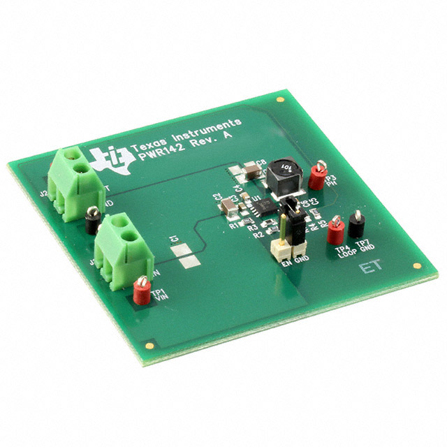
Texas Instruments TPS54061EVM-142TPS54061 - DC/DC, Step Down 1, Non-Isolated Outputs Evaluation Board | 200 mA | DC/DC, Step Down | 60 V | 8 V | 400 kHz | Non-Isolated | 1 | Fully Populated | 3.3 V | Board(s) | TPS54061 |
Description
General part information
TPS54061 Series
The TPS54061-Q1 device is a 60-V, 200-mA, synchronous step-down DC-DC converter with integrated high-side and low-side MOSFETs. Current-mode control provides simple external compensation and flexible component selection. The non-switching supply current is 90 µA. Using the enable pin reduces the shutdown supply current to 1.4 µA.
To increase light-load efficiency, the low-side MOSFET emulates a diode when the inductor current reaches zero.
The internal undervoltage lockout setting is 4.5 V, but using two resistors on the enable pin can increase the setting. The internal slow-start time controls the output-voltage start-up ramp.
Documents
Technical documentation and resources