TLV2544CPW
Obsolete12-BIT 200 KSPS ADC SER. OUT, AUTO PWRDN (S/W AND H/W), LOW POWER W/8 X FIFO W/4 CH.
TLV2544CPW
Obsolete12-BIT 200 KSPS ADC SER. OUT, AUTO PWRDN (S/W AND H/W), LOW POWER W/8 X FIFO W/4 CH.
Description
General part information
TLV2544 Series
The TLV2544Q, TLV2548Q, and TLV2548M are a family of high performance, 12-bit low power, 3.5 µs, CMOS analog-to-digital converters (ADC) which operate from a single 3-V to 5.5-V power supply. These devices have three digital inputs and a 3-state output [chip select (CS), serial input-output clock (SCLK), serial data input (SDI), and serial data output (SDO)] that provide a direct 4-wire interface to the serial port of most popular host microprocessors (SPI interface). When interfaced with a DSP, a frame sync (FS) signal is used to indicate the start of a serial data frame.
In addition to a high-speed A/D converter and versatile control capability, these devices have an on-chip analog multiplexer that can select any analog inputs or one of three internal self-test voltages. The sample-and-hold function is automatically started after the fourth SCLK edge (normal sampling) or can be controlled by a special pin,CSTART, to extend the sampling period (extended sampling). The normal sampling period can also be programmed as short (12 SCLKs) or as long (24 SCLKs) to accommodate faster SCLK operation popular among high-performance signal processors. The TLV2548 and TLV2544 are designed to operate with very low power consumption. The power-saving feature is further enhanced with software/hardware/autopower-down modes and programmable conversion speeds. The conversion clock (OSC) and reference are built-in. The converter can use the external SCLK as the source of the conversion clock to achieve higher (up to 2.8 µs when a 20 MHz SCLK is used) conversion speed. Two different internal reference voltages are available. An optional external reference can also be used to achieve maximum flexibility.
The TLV2544Q and the TLV2548Q are characterized for operation from –40°C to 125°C. The TLV2548M is characterized for operation from –55°C to 125°C.
Technical Specifications
Parameters and characteristics for this part
| Specification | TLV2544CPW |
|---|---|
| Architecture | SAR |
| Configuration | MUX-S/H-ADC |
| Data Interface | DSP, SPI |
| Input Type | Single Ended |
| Mounting Type | Surface Mount |
| Number of A/D Converters | 1 count |
| Number of Bits | 12 bits |
| Number of Inputs | 4 |
| Operating Temperature (Max) | 70 °C |
| Operating Temperature (Min) | 0 °C |
| Package Length | 0.173 in |
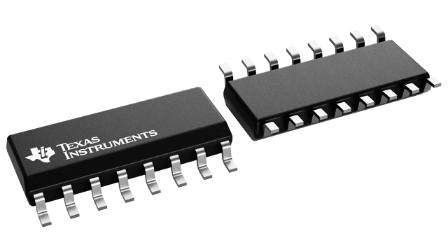
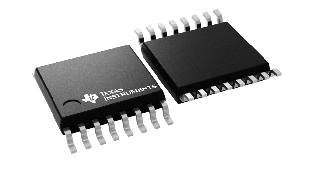
| Package Name | 16-TSSOP |
| Package Width | 4.4 mm |
| Ratio - ADC | 1 |
| Ratio - S/H | 1 |
| Reference Type | External, Internal |
| Sampling Rate (Per Second) | 200 kHz |
| Voltage - Supply, Analog (Max) | 5.5 V |
| Voltage - Supply, Analog (Min) | 2.7 V |
| Voltage - Supply, Digital (Max) | 5.5 V |
| Voltage - Supply, Digital (Min) | 2.7 V |
Pricing
Prices provided here are for design reference only. For realtime values and availability, please visit the distributors directly
Sign in to see pricing
Create a free account to access distributor pricing data.
CAD
3D models and CAD resources for this part
Documents
Technical documentation and resources