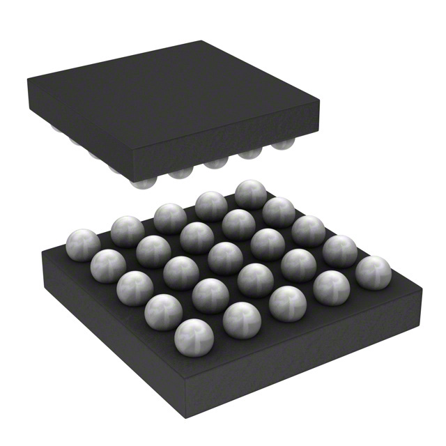
ST6G3244MEBJR
ObsoleteLEVEL TRANSLATOR, 6 INPUT, 7 NS, 1.62 V TO 1.98 V, 25 PINS, FLIP CHIP
Deep-Dive with AI
Search across all available documentation for this part.

ST6G3244MEBJR
ObsoleteLEVEL TRANSLATOR, 6 INPUT, 7 NS, 1.62 V TO 1.98 V, 25 PINS, FLIP CHIP
Deep-Dive with AI
Technical Specifications
Parameters and characteristics for this part
| Specification | ST6G3244MEBJR |
|---|---|
| Channel Type | Bidirectional |
| Data Rate | 120 Mbps |
| Features | Auto-Direction Sensing |
| Mounting Type | Surface Mount |
| Number of Circuits | 1 |
| Operating Temperature [Max] | 85 °C |
| Operating Temperature [Min] | -40 °C |
| Package / Case | FCBGA, 25-UFBGA |
| Supplier Device Package | 25-Flipchip (2x2) |
| Translator Type | Voltage Level |
| Voltage - VCCA [Max] [custom] | 1.98 V |
| Voltage - VCCA [Min] [custom] | 1.62 V |
| Voltage - VCCB [Max] | 2.9 V |
| Voltage - VCCB [Min] | 1.8 V |
Pricing
Prices provided here are for design reference only. For realtime values and availability, please visit the distributors directly
| Distributor | Package | Quantity | $ | |
|---|---|---|---|---|
Description
General part information
ST6G3244 Series
The ST6G3244ME is a dual supply, low voltage 6-bit bi-directional CMOS level translator for SD, mini SD and micro SD Cards. Designed for use as an interface between baseband and memory cards, it achieves high speed operation while maintaining CMOS low-power dissipation.The A-port is designed to track VCCA. The internal LDO is powered by VBATand provides a power supply of either 1.8 V or 2.9 V to the B-side I/Os (programmed by the SEL pin). The B-port is designed to track VCCB. The VCCBvoltage can be also used externally. When VCCB= 0 V, there is no additional leakage seen on VCCA. All outputs are push-pull type.This device is intended for two-way asynchronous communication between data buses. The direction of data transmission is determined by CMD.dir, DAT0.dir and DAT123.dir inputs.All inputs are equipped with protection circuits against electrostatic discharge, giving them ±2 kV (on A-side) and ±15 kV (on B-side, CD and WP) ESD and transient excess voltage immunity.Supports 60 MHz clock rateSupports DDR mode for SD Card™Compliant withSD Specification Part 1 Physical Layer Specification 3.00 (SDR12, SDR25, DDR50)SD Specification Part 1 Physical Layer Specification 2.00Bi-directional with direction control pinBalanced propagation delays: tPLH˜ tPHLLDO power-down support. When the LDO is powered down, VCCBis pulled to GND via the 130 O resistor. When VCCB= 0 V, there is no additional leakage seen on VCCA.EMI filtering and signal conditioningSupports both 1.8 V and 2.9 V data translation on card sideIntegrated LDO to supply 1.8 V or 2.9 V power for B-side I/Os (pin-selectable); can be used also externallyIntegrated pull-up and pull-down resistors on B-sideOperating voltage rangeVCCA= 1.62 V to 1.98 VVBAT= 3.0 V to 5.0 VLatch-up
Documents
Technical documentation and resources


