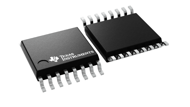
CD74HC137PW
ActiveHIGH SPEED CMOS LOGIC 3-TO-8 LINE DECODER DEMULTIPLEXER WITH ADDRESS LATCHES
Deep-Dive with AI
Search across all available documentation for this part.

CD74HC137PW
ActiveHIGH SPEED CMOS LOGIC 3-TO-8 LINE DECODER DEMULTIPLEXER WITH ADDRESS LATCHES
Deep-Dive with AI
Technical Specifications
Parameters and characteristics commom to parts in this series
| Specification | CD74HC137PW | CD74HC137 Series |
|---|---|---|
| Circuit | 1 x 3:8 | 1 x 3:8 |
| Current - Output High, Low | 5.2 mA, 5.2 mA | 5.2 mA |
| Independent Circuits | 1 | 1 |
| Mounting Type | Surface Mount | Surface Mount, Through Hole |
| Operating Temperature [Max] | 125 °C | 125 °C |
| Operating Temperature [Min] | -55 °C | -55 °C |
| Package / Case | 16-TSSOP | 16-TSSOP, 16-DIP |
| Package / Case | - | 0.3 - 7.62 in |
| Package / Case [x] | 0.173 " | 0.173 " |
| Package / Case [x] | 4.4 mm | 4.4 mm |
| Supplier Device Package | 16-TSSOP | 16-TSSOP, 16-PDIP |
| Type | Decoder/Demultiplexer | Decoder/Demultiplexer |
| Voltage - Supply [Max] | 6 V | 6 V |
| Voltage - Supply [Min] | 2 V | 2 V |
| Voltage Supply Source | Single Supply | Single Supply |
Pricing
Prices provided here are for design reference only. For realtime values and availability, please visit the distributors directly
CD74HC137 Series
High Speed CMOS Logic 3-to-8 Line Decoder Demultiplexer with Address Latches
| Part | Package / Case [x] | Package / Case | Package / Case [x] | Supplier Device Package | Mounting Type | Independent Circuits | Voltage - Supply [Min] | Voltage - Supply [Max] | Type | Operating Temperature [Min] | Operating Temperature [Max] | Voltage Supply Source | Current - Output High, Low | Circuit | Package / Case |
|---|---|---|---|---|---|---|---|---|---|---|---|---|---|---|---|
Texas Instruments CD74HC137PWRThe CD74HC137, CD74HCT137, ’HC237, and CD74HCT237 are high speed silicon gate CMOS decoders well suited to memory address decoding or data routing applications. Both circuits feature low power consumption usually associated with CMOS circuitry, yet have speeds comparable to low power Schottky TTL logic.
Both circuits have three binary select inputs (A0, A1 and A2) that can be latched by an active High Latch Enable (LE) signal to isolate the outputs from select-input changes. A "Low" LE makes the output transparent to the input and the circuit functions as a one-of-eight decoder. Two Output Enable inputs (OE\1and OE0) are provided to simplify cascading and to facilitate demultiplexing. The demultiplexing function is accomplished by using the A0, A1, A2inputs to select the desired output and using one of the other Output Enable inputs as the data input while holding the other Output Enable input in its active state. In the CD74HC137 and CD74HCT137 the selected output is a "Low"; in the ’HC237 and CD74HCT237 the selected output is a "High".
The CD74HC137, CD74HCT137, ’HC237, and CD74HCT237 are high speed silicon gate CMOS decoders well suited to memory address decoding or data routing applications. Both circuits feature low power consumption usually associated with CMOS circuitry, yet have speeds comparable to low power Schottky TTL logic.
Both circuits have three binary select inputs (A0, A1 and A2) that can be latched by an active High Latch Enable (LE) signal to isolate the outputs from select-input changes. A "Low" LE makes the output transparent to the input and the circuit functions as a one-of-eight decoder. Two Output Enable inputs (OE\1and OE0) are provided to simplify cascading and to facilitate demultiplexing. The demultiplexing function is accomplished by using the A0, A1, A2inputs to select the desired output and using one of the other Output Enable inputs as the data input while holding the other Output Enable input in its active state. In the CD74HC137 and CD74HCT137 the selected output is a "Low"; in the ’HC237 and CD74HCT237 the selected output is a "High". | 0.173 " | 16-TSSOP | 4.4 mm | 16-TSSOP | Surface Mount | 1 | 2 V | 6 V | Decoder/Demultiplexer | -55 °C | 125 °C | Single Supply | 5.2 mA, 5.2 mA | 1 x 3:8 | |
Texas Instruments CD74HC137EThe CD74HC137, CD74HCT137, ’HC237, and CD74HCT237 are high speed silicon gate CMOS decoders well suited to memory address decoding or data routing applications. Both circuits feature low power consumption usually associated with CMOS circuitry, yet have speeds comparable to low power Schottky TTL logic.
Both circuits have three binary select inputs (A0, A1 and A2) that can be latched by an active High Latch Enable (LE) signal to isolate the outputs from select-input changes. A "Low" LE makes the output transparent to the input and the circuit functions as a one-of-eight decoder. Two Output Enable inputs (OE\1and OE0) are provided to simplify cascading and to facilitate demultiplexing. The demultiplexing function is accomplished by using the A0, A1, A2inputs to select the desired output and using one of the other Output Enable inputs as the data input while holding the other Output Enable input in its active state. In the CD74HC137 and CD74HCT137 the selected output is a "Low"; in the ’HC237 and CD74HCT237 the selected output is a "High".
The CD74HC137, CD74HCT137, ’HC237, and CD74HCT237 are high speed silicon gate CMOS decoders well suited to memory address decoding or data routing applications. Both circuits feature low power consumption usually associated with CMOS circuitry, yet have speeds comparable to low power Schottky TTL logic.
Both circuits have three binary select inputs (A0, A1 and A2) that can be latched by an active High Latch Enable (LE) signal to isolate the outputs from select-input changes. A "Low" LE makes the output transparent to the input and the circuit functions as a one-of-eight decoder. Two Output Enable inputs (OE\1and OE0) are provided to simplify cascading and to facilitate demultiplexing. The demultiplexing function is accomplished by using the A0, A1, A2inputs to select the desired output and using one of the other Output Enable inputs as the data input while holding the other Output Enable input in its active state. In the CD74HC137 and CD74HCT137 the selected output is a "Low"; in the ’HC237 and CD74HCT237 the selected output is a "High". | 16-DIP | 16-PDIP | Through Hole | 1 | 2 V | 6 V | Decoder/Demultiplexer | -55 °C | 125 °C | Single Supply | 5.2 mA, 5.2 mA | 1 x 3:8 | 0.3 in, 7.62 mm | ||
Texas Instruments CD74HC137PWThe CD74HC137, CD74HCT137, ’HC237, and CD74HCT237 are high speed silicon gate CMOS decoders well suited to memory address decoding or data routing applications. Both circuits feature low power consumption usually associated with CMOS circuitry, yet have speeds comparable to low power Schottky TTL logic.
Both circuits have three binary select inputs (A0, A1 and A2) that can be latched by an active High Latch Enable (LE) signal to isolate the outputs from select-input changes. A "Low" LE makes the output transparent to the input and the circuit functions as a one-of-eight decoder. Two Output Enable inputs (OE\1and OE0) are provided to simplify cascading and to facilitate demultiplexing. The demultiplexing function is accomplished by using the A0, A1, A2inputs to select the desired output and using one of the other Output Enable inputs as the data input while holding the other Output Enable input in its active state. In the CD74HC137 and CD74HCT137 the selected output is a "Low"; in the ’HC237 and CD74HCT237 the selected output is a "High".
The CD74HC137, CD74HCT137, ’HC237, and CD74HCT237 are high speed silicon gate CMOS decoders well suited to memory address decoding or data routing applications. Both circuits feature low power consumption usually associated with CMOS circuitry, yet have speeds comparable to low power Schottky TTL logic.
Both circuits have three binary select inputs (A0, A1 and A2) that can be latched by an active High Latch Enable (LE) signal to isolate the outputs from select-input changes. A "Low" LE makes the output transparent to the input and the circuit functions as a one-of-eight decoder. Two Output Enable inputs (OE\1and OE0) are provided to simplify cascading and to facilitate demultiplexing. The demultiplexing function is accomplished by using the A0, A1, A2inputs to select the desired output and using one of the other Output Enable inputs as the data input while holding the other Output Enable input in its active state. In the CD74HC137 and CD74HCT137 the selected output is a "Low"; in the ’HC237 and CD74HCT237 the selected output is a "High". | 0.173 " | 16-TSSOP | 4.4 mm | 16-TSSOP | Surface Mount | 1 | 2 V | 6 V | Decoder/Demultiplexer | -55 °C | 125 °C | Single Supply | 5.2 mA, 5.2 mA | 1 x 3:8 |
Description
General part information
CD74HC137 Series
The CD74HC137, CD74HCT137, ’HC237, and CD74HCT237 are high speed silicon gate CMOS decoders well suited to memory address decoding or data routing applications. Both circuits feature low power consumption usually associated with CMOS circuitry, yet have speeds comparable to low power Schottky TTL logic.
Both circuits have three binary select inputs (A0, A1 and A2) that can be latched by an active High Latch Enable (LE) signal to isolate the outputs from select-input changes. A "Low" LE makes the output transparent to the input and the circuit functions as a one-of-eight decoder. Two Output Enable inputs (OE\1and OE0) are provided to simplify cascading and to facilitate demultiplexing. The demultiplexing function is accomplished by using the A0, A1, A2inputs to select the desired output and using one of the other Output Enable inputs as the data input while holding the other Output Enable input in its active state. In the CD74HC137 and CD74HCT137 the selected output is a "Low"; in the ’HC237 and CD74HCT237 the selected output is a "High".
The CD74HC137, CD74HCT137, ’HC237, and CD74HCT237 are high speed silicon gate CMOS decoders well suited to memory address decoding or data routing applications. Both circuits feature low power consumption usually associated with CMOS circuitry, yet have speeds comparable to low power Schottky TTL logic.
Documents
Technical documentation and resources


