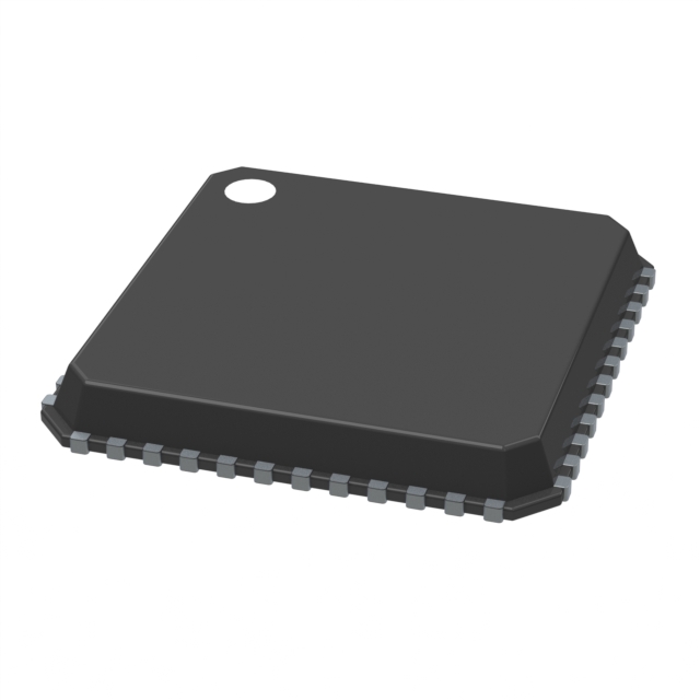
TLE92613BQXV33XUMA2
ActiveTHE TLE9261-3BQXV33 IS A MONOLITHIC INTEGRATED CIRCUIT IN A 7MM X 7MM POWER PACKAGE WITH LEAD TIP INSPECTION (LTI) FEATURE TO SUPPORT AUTOMATIC OPTICAL INSPECTION (AOI)
Deep-Dive with AI
Search across all available documentation for this part.

TLE92613BQXV33XUMA2
ActiveTHE TLE9261-3BQXV33 IS A MONOLITHIC INTEGRATED CIRCUIT IN A 7MM X 7MM POWER PACKAGE WITH LEAD TIP INSPECTION (LTI) FEATURE TO SUPPORT AUTOMATIC OPTICAL INSPECTION (AOI)
Deep-Dive with AI
Technical Specifications
Parameters and characteristics for this part
| Specification | TLE92613BQXV33XUMA2 |
|---|---|
| Applications | System Basis Chip |
| Current - Supply | 3.5 mA |
| Mounting Type | Surface Mount |
| Operating Temperature [Max] | 150 °C |
| Operating Temperature [Min] | -40 °C |
| Package / Case | 48-VFQFN Exposed Pad |
| Supplier Device Package | PG-VQFN-48-79 |
| Voltage - Supply [Max] | 28 V |
| Voltage - Supply [Min] | 3 V |
Pricing
Prices provided here are for design reference only. For realtime values and availability, please visit the distributors directly
| Distributor | Package | Quantity | $ | |
|---|---|---|---|---|
| Digikey | Tape & Reel (TR) | 2500 | $ 2.13 | |
Description
General part information
TLE92613 Series
The TLE9261-3BQXV33 is a monolithic integrated circuit in an exposed pad VQFN-48 (7mm x 7mm) power package with Lead Tip Inspection (LTI) feature to support Automatic Optical Inspection (AOI). The device is designed for various CAN automotive applications as main supply for the microcontroller and as interface for a CAN bus network including the CAN Partial Networking feature. To support these applications, the System Basis Chip (SBC) provides the main functions, such as a 3.3V lowdropout voltage regulator (LDO) for e.g. a microcontroller supply, another 5V low-dropout voltage regulator with off-board protection for e.g. sensor supply, another 3.3V/1.8V regulator to drive an external PNP transistor, which can be used as an independent supply for off-board usage or in load sharing configuration with the main regulator VCC1, a HS-CAN transceiver supporting CAN FD and CAN Partial Networking (incl. FD tolerant mode) for data transmission, high-side switches with embedded protective functions and a 16-bit Serial Peripheral Interface (SPI) to control and monitor the device. Also implemented are a configurable timeout / window watchdog circuit with a reset feature, three Fail Outputs and an undervoltage reset feature. The device offers low-power modes in order to minimize current consumption on applications that are connected permanently to the battery. A wake-up from the low-power mode is possible via a message on the buses, via the bi level sensitive monitoring/wake-up inputs as well as via cyclic wake. The device is designed to withstand the severe conditions of automotive applications.
Documents
Technical documentation and resources


