ISL89164FRTBZ-T
ActiveHIGH SPEED, DUAL CHANNEL, 6A, POWER MOSFET DRIVER WITH ENABLE INPUTS
ISL89164FRTBZ-T
ActiveHIGH SPEED, DUAL CHANNEL, 6A, POWER MOSFET DRIVER WITH ENABLE INPUTS
Description
General part information
ISL89164 Series
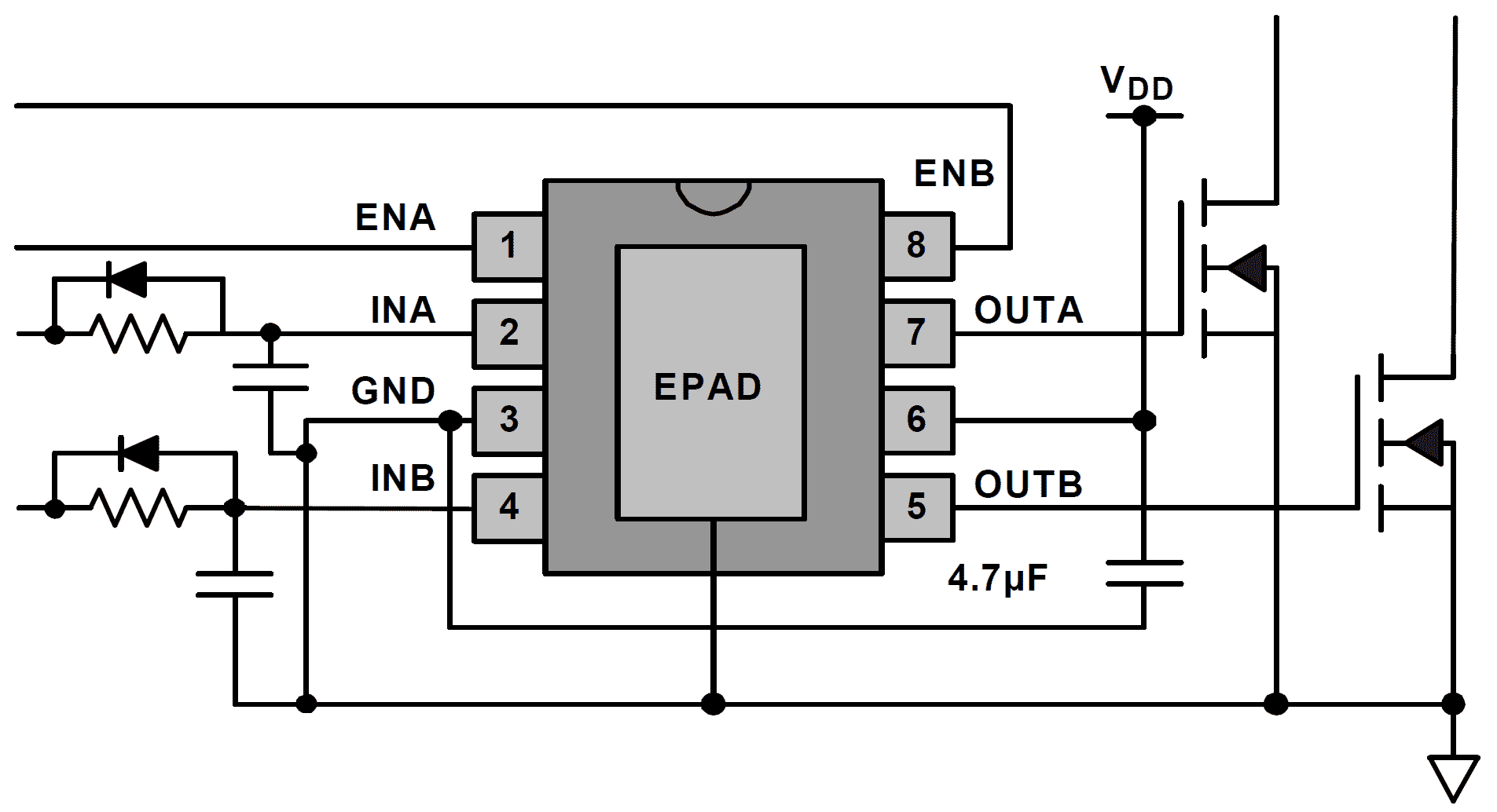
The ISL89163, ISL89164, and ISL89165 are high-speed, 6A, dual channel MOSFET drivers with enable inputs. Precision thresholds on all logic inputs allow the use of external RC circuits to generate accurate and stable time delays on both the main channel inputs, INA and INB, and the enable inputs, ENA and ENB. The precision delays capable of these precise logic thresholds makes these parts very useful for dead-time control and synchronous rectifiers. Note that the enable and input logic inputs can be interchanged for alternate logic implementations. Three input logic thresholds are available: 3. 3V (CMOS), 5. 0V (CMOS or TTL compatible), and CMOS thresholds that are proportional to VDD. At high switching frequencies, these MOSFET drivers use very little internal bias currents. Separate, non-overlapping drive circuits are used to drive each CMOS output FET to prevent shoot-through currents in the output stage. The start-up sequence is designed to prevent unexpected glitches when VDDis being turned on or turned off. When VDD~1V, an internal 10kΩ resistor between the output and ground helps to keep the output voltage low. When ~1V VDDUV, both outputs are driven low with very low resistance and the logic inputs are ignored. This insures that the driven FETs are off. When VDD> UVLO, and after a short delay, the outputs now respond to the logic inputs.
Technical Specifications
Parameters and characteristics for this part
| Specification | ISL89164FRTBZ-T |
|---|---|
| Channel Type | Independent |
| Current - Peak Output (Sink) | 6 A |
| Current - Peak Output (Source) | 6 A |
| Driven Configuration | Low-Side |
| Fall Time (Typ) | 20 ns |
| Gate Channel | N-Channel |
| Gate Type | MOSFET |
| Input Type | Inverting |
| Logic Voltage - VIH | 3.15 V |
| Logic Voltage - VIL | 1.85 V |
| Mounting Type | Surface Mount |
| Number of Drivers | 2 |
| Operating Temperature (Max) | 125 °C |
| Operating Temperature (Min) | -40 °C |
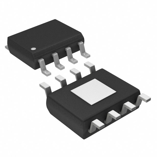
| Package / Case | 8-WDFN Exposed Pad |
| Package Length | 3 mm |
| Package Name | 8-TDFN |
| Package Width | 3 mm |
| Rise Time (Typ) | 20 ns |
| Voltage - Supply (Maximum) | 16 V |
| Voltage - Supply (Minimum) | 4.5 V |
Pricing
Prices provided here are for design reference only. For realtime values and availability, please visit the distributors directly
Sign in to see pricing
Create a free account to access distributor pricing data.
CAD
3D models and CAD resources for this part
Documents
Technical documentation and resources