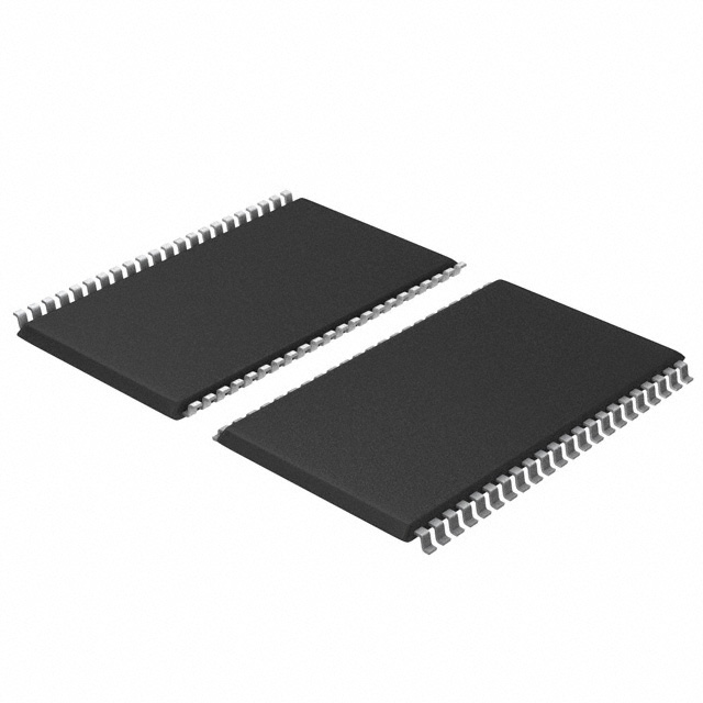
CY7C1020DV33-10ZSXI
ActiveSRAM, ASYNCHRONOUS SRAM, 512 KBIT, 32K X 16BIT, TSOP, 44 PINS, 3 V
Deep-Dive with AI
Search across all available documentation for this part.

CY7C1020DV33-10ZSXI
ActiveSRAM, ASYNCHRONOUS SRAM, 512 KBIT, 32K X 16BIT, TSOP, 44 PINS, 3 V
Deep-Dive with AI
Technical Specifications
Parameters and characteristics for this part
| Specification | CY7C1020DV33-10ZSXI |
|---|---|
| Access Time | 10 ns |
| Memory Format | SRAM |
| Memory Interface | Parallel |
| Memory Size | 64 kb |
| Memory Type | Volatile |
| Mounting Type | Surface Mount |
| Operating Temperature [Max] | 85 °C |
| Operating Temperature [Min] | -40 °C |
| Package / Case | 10.16 mm |
| Package / Case | 10.16 mm |
| Package / Case | 44-TSOP |
| Supplier Device Package | 44-TSOP II |
| Technology | SRAM - Asynchronous |
| Voltage - Supply [Max] | 3.6 V |
| Voltage - Supply [Min] | 3 V |
| Write Cycle Time - Word, Page | 10 ns |
Pricing
Prices provided here are for design reference only. For realtime values and availability, please visit the distributors directly
Description
General part information
CY7C1020 Series
CY7C1020DV33-10ZSXI is a CY7C1020DV33 high-performance CMOS static RAM organized as 32,768 words by 16 bits. This device has an automatic power-down feature that significantly reduces power consumption when deselected. Writing to the device is accomplished by taking chip enable (CE) and write enable (WE) inputs low. If byte low enable (BLE) is low, then data from I/O pins (I/O0 through I/O7), is written into the location specified on the address pins (A0 through A14). If byte high enable (BHE) is LOW, then data from I/O pins (I/O8 through I/O15) is written into the location specified on the address pins (A0 through A14). Reading from the device is accomplished by taking chip enable active-low (CE) and output enable (OE) low while forcing the write enable (WE) high. If byte low enable (BLE) is low, then data from the memory location specified by the address pins will appear on I/O0 to I/O7. If byte high enable (BHE) is low, then data from memory will appear on I/O8 to I/O15.
Documents
Technical documentation and resources


