TPS70258PWPR
Active500-MA, DUAL-CHANNEL LOW-DROPOUT VOLTAGE REGULATOR WITH POWER GOOD & INDEPENDENT ENABLE
Deep-Dive with AI
Search across all available documentation for this part.
TPS70258PWPR
Active500-MA, DUAL-CHANNEL LOW-DROPOUT VOLTAGE REGULATOR WITH POWER GOOD & INDEPENDENT ENABLE
Deep-Dive with AI
Technical Specifications
Parameters and characteristics commom to parts in this series
| Specification | TPS70258PWPR | TPS702 Series |
|---|---|---|
| Control Features | Power Good, Sequencing, Enable, Reset | Power Good, Sequencing, Enable, Reset |
| Current - Output | 250 mA, 500 mA | 250 - 500 mA |
| Current - Quiescent (Iq) | 190 çA | 190 çA |
| Current - Supply (Max) [Max] | 230 µA | 230 µA |
| Mounting Type | Surface Mount | Surface Mount |
| Number of Regulators | 2 | 2 |
| Operating Temperature [Max] | 125 °C | 125 °C |
| Operating Temperature [Min] | -40 °C | -40 °C |
| Output Configuration | Positive | Positive |
| Output Type | 27.03 °C/W | 27.03 °C/W |
| Output Type | - | Adjustable |
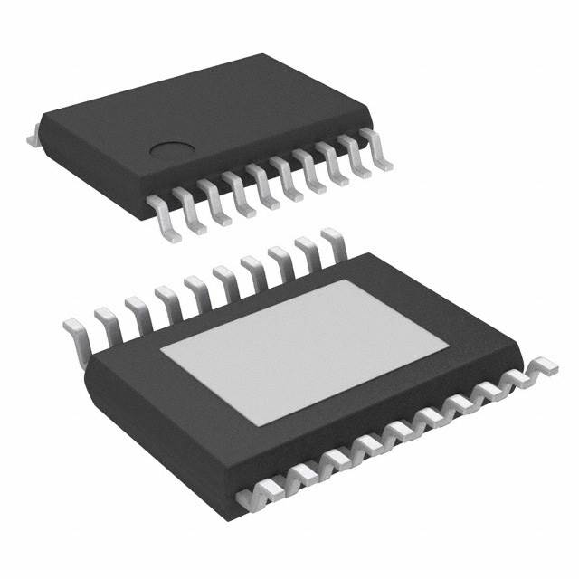
| Package / Case | 20-PowerTSSOP | 20-PowerTSSOP |
| Package / Case [custom] | 0.173 in | 0.173 in |
| Package / Case [custom] | 4.4 mm | 4.4 mm |
| Protection Features | Over Current, Reverse Polarity, Under Voltage Lockout (UVLO), Over Temperature | Over Current, Reverse Polarity, Under Voltage Lockout (UVLO), Over Temperature |
| PSRR | 50 dB, 60 dB | 50 - 60 dB |
| Supplier Device Package | 20-HTSSOP | 20-HTSSOP |
| Voltage - Input (Max) [Max] | 6 V | 6 V |
| Voltage - Output (Max) | - | 5.5 V |
| Voltage - Output (Min/Fixed) | 2.5 V | 1.2 - 2.5 V |
| Voltage - Output (Min/Fixed) [Min] | 3.3 V | 3.3 V |
| Voltage Dropout (Max) [Max] | 0.28 V | 0.28 V |
Pricing
Prices provided here are for design reference only. For realtime values and availability, please visit the distributors directly
TPS702 Series
500-mA, dual-channel low-dropout voltage regulator with power good & independent enable
| Part | Voltage - Output (Min/Fixed) | Voltage - Output (Min/Fixed) [Min] | Voltage Dropout (Max) [Max] | Operating Temperature [Max] | Operating Temperature [Min] | Output Type | Number of Regulators | Output Configuration | Current - Quiescent (Iq) | Voltage - Input (Max) [Max] | Current - Output | Current - Supply (Max) [Max] | Control Features | Supplier Device Package | Mounting Type | PSRR | Package / Case [custom] | Package / Case | Package / Case [custom] | Protection Features | Voltage - Output (Max) [Max] | Output Type |
|---|---|---|---|---|---|---|---|---|---|---|---|---|---|---|---|---|---|---|---|---|---|---|
Texas Instruments TPS70251PWPRThe TPS702xx is a low dropout voltage regulator with integrated SVS (RESET, POR, or power on reset) and power good (PG) functions. These devices are capable of supplying 500mA and 250mA by regulator 1 and regulator 2 respectively. Quiescent current is typically 190µA at full load. Differentiated features, such as accuracy, fast transient response, SVS supervisory circuit (power on reset), manual reset input, and independent enable functions provide a complete system solution.
The TPS702xx family of voltage regulators offers very low dropout voltage and dual outputs. These devices have extremely low noise output performance without using any added filter bypass capacitors and are designed to have a fast transient response and be stable with 10µF low ESR capacitors.
These devices have fixed 3.3V/2.5V, 3.3V/1.8V, 3.3V/1.5V, 3.3V/1.2V, and adjustable voltage options. Regulator 1 can support up to 500mA, and regulator 2 can support up to 250mA. Separate voltage inputs allow the designer to configure the source power.
Because the PMOS device behaves as a low-value resistor, the dropout voltage is very low (typically 170mV on regulator 1) and is directly proportional to the output current. Additionally, since the PMOS pass element is a voltage-driven device, the quiescent current is very low and independent of output loading (maximum of 230µA over the full range of output current and full range of temperature). This LDO family also features a sleep mode; applying a high signal toEN1orEN2(enable) shuts down regulator 1 or regulator 2, respectively. When a high signal is applied to bothEN1andEN2, both regulators enter sleep mode, thereby reducing the input current to 2µA at TJ= +25°C.
For each regulator, there is an internal discharge transistor to discharge the output capacitor when the regulator is turned off (disabled).
The PG1 pin reports the voltage condition at VOUT1. The PG1 pin can be used to implement a SVS (RESET, POR, or power on reset) for the circuitry supplied by regulator 1. The PG2 pin reports the voltage conditions at VOUT2. The PG2 pin can be used to implement a SVS (power on reset) for the circuitry supplied by regulator 2.
The TPS702xx features aRESET(SVS, POR, or power on reset).RESEToutput initiates a reset in the event of an undervoltage condition.RESETalso indicates the status of the manual reset pin (MR). WhenMRis in the logic high state,RESETgoes to a high impedance state after a 120ms delay. To monitor VOUT1, the PG1 output pin can be connected toMR. To monitor VOUT2, the PG2 output pin can be connected toMR.
The device has an undervoltage lockout UVLO circuit that prevents the internal regulators from turning on until VIN1reaches 2.5V.
The TPS702xx is a low dropout voltage regulator with integrated SVS (RESET, POR, or power on reset) and power good (PG) functions. These devices are capable of supplying 500mA and 250mA by regulator 1 and regulator 2 respectively. Quiescent current is typically 190µA at full load. Differentiated features, such as accuracy, fast transient response, SVS supervisory circuit (power on reset), manual reset input, and independent enable functions provide a complete system solution.
The TPS702xx family of voltage regulators offers very low dropout voltage and dual outputs. These devices have extremely low noise output performance without using any added filter bypass capacitors and are designed to have a fast transient response and be stable with 10µF low ESR capacitors.
These devices have fixed 3.3V/2.5V, 3.3V/1.8V, 3.3V/1.5V, 3.3V/1.2V, and adjustable voltage options. Regulator 1 can support up to 500mA, and regulator 2 can support up to 250mA. Separate voltage inputs allow the designer to configure the source power.
Because the PMOS device behaves as a low-value resistor, the dropout voltage is very low (typically 170mV on regulator 1) and is directly proportional to the output current. Additionally, since the PMOS pass element is a voltage-driven device, the quiescent current is very low and independent of output loading (maximum of 230µA over the full range of output current and full range of temperature). This LDO family also features a sleep mode; applying a high signal toEN1orEN2(enable) shuts down regulator 1 or regulator 2, respectively. When a high signal is applied to bothEN1andEN2, both regulators enter sleep mode, thereby reducing the input current to 2µA at TJ= +25°C.
For each regulator, there is an internal discharge transistor to discharge the output capacitor when the regulator is turned off (disabled).
The PG1 pin reports the voltage condition at VOUT1. The PG1 pin can be used to implement a SVS (RESET, POR, or power on reset) for the circuitry supplied by regulator 1. The PG2 pin reports the voltage conditions at VOUT2. The PG2 pin can be used to implement a SVS (power on reset) for the circuitry supplied by regulator 2.
The TPS702xx features aRESET(SVS, POR, or power on reset).RESEToutput initiates a reset in the event of an undervoltage condition.RESETalso indicates the status of the manual reset pin (MR). WhenMRis in the logic high state,RESETgoes to a high impedance state after a 120ms delay. To monitor VOUT1, the PG1 output pin can be connected toMR. To monitor VOUT2, the PG2 output pin can be connected toMR.
The device has an undervoltage lockout UVLO circuit that prevents the internal regulators from turning on until VIN1reaches 2.5V. | 1.8 V | 3.3 V | 0.28 V | 125 °C | -40 °C | 27.03 °C/W | 2 | Positive | 190 çA | 6 V | 250 mA, 500 mA | 230 µA | Enable, Power Good, Reset, Sequencing | 20-HTSSOP | Surface Mount | 50 dB, 60 dB | 0.173 in | 20-PowerTSSOP | 4.4 mm | Over Current, Over Temperature, Reverse Polarity, Under Voltage Lockout (UVLO) | ||
Texas Instruments TPS70258PWPThe TPS702xx is a low dropout voltage regulator with integrated SVS (RESET, POR, or power on reset) and power good (PG) functions. These devices are capable of supplying 500mA and 250mA by regulator 1 and regulator 2 respectively. Quiescent current is typically 190µA at full load. Differentiated features, such as accuracy, fast transient response, SVS supervisory circuit (power on reset), manual reset input, and independent enable functions provide a complete system solution.
The TPS702xx family of voltage regulators offers very low dropout voltage and dual outputs. These devices have extremely low noise output performance without using any added filter bypass capacitors and are designed to have a fast transient response and be stable with 10µF low ESR capacitors.
These devices have fixed 3.3V/2.5V, 3.3V/1.8V, 3.3V/1.5V, 3.3V/1.2V, and adjustable voltage options. Regulator 1 can support up to 500mA, and regulator 2 can support up to 250mA. Separate voltage inputs allow the designer to configure the source power.
Because the PMOS device behaves as a low-value resistor, the dropout voltage is very low (typically 170mV on regulator 1) and is directly proportional to the output current. Additionally, since the PMOS pass element is a voltage-driven device, the quiescent current is very low and independent of output loading (maximum of 230µA over the full range of output current and full range of temperature). This LDO family also features a sleep mode; applying a high signal toEN1orEN2(enable) shuts down regulator 1 or regulator 2, respectively. When a high signal is applied to bothEN1andEN2, both regulators enter sleep mode, thereby reducing the input current to 2µA at TJ= +25°C.
For each regulator, there is an internal discharge transistor to discharge the output capacitor when the regulator is turned off (disabled).
The PG1 pin reports the voltage condition at VOUT1. The PG1 pin can be used to implement a SVS (RESET, POR, or power on reset) for the circuitry supplied by regulator 1. The PG2 pin reports the voltage conditions at VOUT2. The PG2 pin can be used to implement a SVS (power on reset) for the circuitry supplied by regulator 2.
The TPS702xx features aRESET(SVS, POR, or power on reset).RESEToutput initiates a reset in the event of an undervoltage condition.RESETalso indicates the status of the manual reset pin (MR). WhenMRis in the logic high state,RESETgoes to a high impedance state after a 120ms delay. To monitor VOUT1, the PG1 output pin can be connected toMR. To monitor VOUT2, the PG2 output pin can be connected toMR.
The device has an undervoltage lockout UVLO circuit that prevents the internal regulators from turning on until VIN1reaches 2.5V.
The TPS702xx is a low dropout voltage regulator with integrated SVS (RESET, POR, or power on reset) and power good (PG) functions. These devices are capable of supplying 500mA and 250mA by regulator 1 and regulator 2 respectively. Quiescent current is typically 190µA at full load. Differentiated features, such as accuracy, fast transient response, SVS supervisory circuit (power on reset), manual reset input, and independent enable functions provide a complete system solution.
The TPS702xx family of voltage regulators offers very low dropout voltage and dual outputs. These devices have extremely low noise output performance without using any added filter bypass capacitors and are designed to have a fast transient response and be stable with 10µF low ESR capacitors.
These devices have fixed 3.3V/2.5V, 3.3V/1.8V, 3.3V/1.5V, 3.3V/1.2V, and adjustable voltage options. Regulator 1 can support up to 500mA, and regulator 2 can support up to 250mA. Separate voltage inputs allow the designer to configure the source power.
Because the PMOS device behaves as a low-value resistor, the dropout voltage is very low (typically 170mV on regulator 1) and is directly proportional to the output current. Additionally, since the PMOS pass element is a voltage-driven device, the quiescent current is very low and independent of output loading (maximum of 230µA over the full range of output current and full range of temperature). This LDO family also features a sleep mode; applying a high signal toEN1orEN2(enable) shuts down regulator 1 or regulator 2, respectively. When a high signal is applied to bothEN1andEN2, both regulators enter sleep mode, thereby reducing the input current to 2µA at TJ= +25°C.
For each regulator, there is an internal discharge transistor to discharge the output capacitor when the regulator is turned off (disabled).
The PG1 pin reports the voltage condition at VOUT1. The PG1 pin can be used to implement a SVS (RESET, POR, or power on reset) for the circuitry supplied by regulator 1. The PG2 pin reports the voltage conditions at VOUT2. The PG2 pin can be used to implement a SVS (power on reset) for the circuitry supplied by regulator 2.
The TPS702xx features aRESET(SVS, POR, or power on reset).RESEToutput initiates a reset in the event of an undervoltage condition.RESETalso indicates the status of the manual reset pin (MR). WhenMRis in the logic high state,RESETgoes to a high impedance state after a 120ms delay. To monitor VOUT1, the PG1 output pin can be connected toMR. To monitor VOUT2, the PG2 output pin can be connected toMR.
The device has an undervoltage lockout UVLO circuit that prevents the internal regulators from turning on until VIN1reaches 2.5V. | 2.5 V | 3.3 V | 0.28 V | 125 °C | -40 °C | 27.03 °C/W | 2 | Positive | 190 çA | 6 V | 250 mA, 500 mA | 230 µA | Enable, Power Good, Reset, Sequencing | 20-HTSSOP | Surface Mount | 50 dB, 60 dB | 0.173 in | 20-PowerTSSOP | 4.4 mm | Over Current, Over Temperature, Reverse Polarity, Under Voltage Lockout (UVLO) | ||
Texas Instruments TPS70248PWPThe TPS702xx is a low dropout voltage regulator with integrated SVS (RESET, POR, or power on reset) and power good (PG) functions. These devices are capable of supplying 500mA and 250mA by regulator 1 and regulator 2 respectively. Quiescent current is typically 190µA at full load. Differentiated features, such as accuracy, fast transient response, SVS supervisory circuit (power on reset), manual reset input, and independent enable functions provide a complete system solution.
The TPS702xx family of voltage regulators offers very low dropout voltage and dual outputs. These devices have extremely low noise output performance without using any added filter bypass capacitors and are designed to have a fast transient response and be stable with 10µF low ESR capacitors.
These devices have fixed 3.3V/2.5V, 3.3V/1.8V, 3.3V/1.5V, 3.3V/1.2V, and adjustable voltage options. Regulator 1 can support up to 500mA, and regulator 2 can support up to 250mA. Separate voltage inputs allow the designer to configure the source power.
Because the PMOS device behaves as a low-value resistor, the dropout voltage is very low (typically 170mV on regulator 1) and is directly proportional to the output current. Additionally, since the PMOS pass element is a voltage-driven device, the quiescent current is very low and independent of output loading (maximum of 230µA over the full range of output current and full range of temperature). This LDO family also features a sleep mode; applying a high signal toEN1orEN2(enable) shuts down regulator 1 or regulator 2, respectively. When a high signal is applied to bothEN1andEN2, both regulators enter sleep mode, thereby reducing the input current to 2µA at TJ= +25°C.
For each regulator, there is an internal discharge transistor to discharge the output capacitor when the regulator is turned off (disabled).
The PG1 pin reports the voltage condition at VOUT1. The PG1 pin can be used to implement a SVS (RESET, POR, or power on reset) for the circuitry supplied by regulator 1. The PG2 pin reports the voltage conditions at VOUT2. The PG2 pin can be used to implement a SVS (power on reset) for the circuitry supplied by regulator 2.
The TPS702xx features aRESET(SVS, POR, or power on reset).RESEToutput initiates a reset in the event of an undervoltage condition.RESETalso indicates the status of the manual reset pin (MR). WhenMRis in the logic high state,RESETgoes to a high impedance state after a 120ms delay. To monitor VOUT1, the PG1 output pin can be connected toMR. To monitor VOUT2, the PG2 output pin can be connected toMR.
The device has an undervoltage lockout UVLO circuit that prevents the internal regulators from turning on until VIN1reaches 2.5V.
The TPS702xx is a low dropout voltage regulator with integrated SVS (RESET, POR, or power on reset) and power good (PG) functions. These devices are capable of supplying 500mA and 250mA by regulator 1 and regulator 2 respectively. Quiescent current is typically 190µA at full load. Differentiated features, such as accuracy, fast transient response, SVS supervisory circuit (power on reset), manual reset input, and independent enable functions provide a complete system solution.
The TPS702xx family of voltage regulators offers very low dropout voltage and dual outputs. These devices have extremely low noise output performance without using any added filter bypass capacitors and are designed to have a fast transient response and be stable with 10µF low ESR capacitors.
These devices have fixed 3.3V/2.5V, 3.3V/1.8V, 3.3V/1.5V, 3.3V/1.2V, and adjustable voltage options. Regulator 1 can support up to 500mA, and regulator 2 can support up to 250mA. Separate voltage inputs allow the designer to configure the source power.
Because the PMOS device behaves as a low-value resistor, the dropout voltage is very low (typically 170mV on regulator 1) and is directly proportional to the output current. Additionally, since the PMOS pass element is a voltage-driven device, the quiescent current is very low and independent of output loading (maximum of 230µA over the full range of output current and full range of temperature). This LDO family also features a sleep mode; applying a high signal toEN1orEN2(enable) shuts down regulator 1 or regulator 2, respectively. When a high signal is applied to bothEN1andEN2, both regulators enter sleep mode, thereby reducing the input current to 2µA at TJ= +25°C.
For each regulator, there is an internal discharge transistor to discharge the output capacitor when the regulator is turned off (disabled).
The PG1 pin reports the voltage condition at VOUT1. The PG1 pin can be used to implement a SVS (RESET, POR, or power on reset) for the circuitry supplied by regulator 1. The PG2 pin reports the voltage conditions at VOUT2. The PG2 pin can be used to implement a SVS (power on reset) for the circuitry supplied by regulator 2.
The TPS702xx features aRESET(SVS, POR, or power on reset).RESEToutput initiates a reset in the event of an undervoltage condition.RESETalso indicates the status of the manual reset pin (MR). WhenMRis in the logic high state,RESETgoes to a high impedance state after a 120ms delay. To monitor VOUT1, the PG1 output pin can be connected toMR. To monitor VOUT2, the PG2 output pin can be connected toMR.
The device has an undervoltage lockout UVLO circuit that prevents the internal regulators from turning on until VIN1reaches 2.5V. | 1.5 V | 3.3 V | 0.28 V | 125 °C | -40 °C | 27.03 °C/W | 2 | Positive | 190 çA | 6 V | 250 mA, 500 mA | 230 µA | Enable, Power Good, Reset, Sequencing | 20-HTSSOP | Surface Mount | 50 dB, 60 dB | 0.173 in | 20-PowerTSSOP | 4.4 mm | Over Current, Over Temperature, Reverse Polarity, Under Voltage Lockout (UVLO) | ||
Texas Instruments TPS70245PWPRThe TPS702xx is a low dropout voltage regulator with integrated SVS (RESET, POR, or power on reset) and power good (PG) functions. These devices are capable of supplying 500mA and 250mA by regulator 1 and regulator 2 respectively. Quiescent current is typically 190µA at full load. Differentiated features, such as accuracy, fast transient response, SVS supervisory circuit (power on reset), manual reset input, and independent enable functions provide a complete system solution.
The TPS702xx family of voltage regulators offers very low dropout voltage and dual outputs. These devices have extremely low noise output performance without using any added filter bypass capacitors and are designed to have a fast transient response and be stable with 10µF low ESR capacitors.
These devices have fixed 3.3V/2.5V, 3.3V/1.8V, 3.3V/1.5V, 3.3V/1.2V, and adjustable voltage options. Regulator 1 can support up to 500mA, and regulator 2 can support up to 250mA. Separate voltage inputs allow the designer to configure the source power.
Because the PMOS device behaves as a low-value resistor, the dropout voltage is very low (typically 170mV on regulator 1) and is directly proportional to the output current. Additionally, since the PMOS pass element is a voltage-driven device, the quiescent current is very low and independent of output loading (maximum of 230µA over the full range of output current and full range of temperature). This LDO family also features a sleep mode; applying a high signal toEN1orEN2(enable) shuts down regulator 1 or regulator 2, respectively. When a high signal is applied to bothEN1andEN2, both regulators enter sleep mode, thereby reducing the input current to 2µA at TJ= +25°C.
For each regulator, there is an internal discharge transistor to discharge the output capacitor when the regulator is turned off (disabled).
The PG1 pin reports the voltage condition at VOUT1. The PG1 pin can be used to implement a SVS (RESET, POR, or power on reset) for the circuitry supplied by regulator 1. The PG2 pin reports the voltage conditions at VOUT2. The PG2 pin can be used to implement a SVS (power on reset) for the circuitry supplied by regulator 2.
The TPS702xx features aRESET(SVS, POR, or power on reset).RESEToutput initiates a reset in the event of an undervoltage condition.RESETalso indicates the status of the manual reset pin (MR). WhenMRis in the logic high state,RESETgoes to a high impedance state after a 120ms delay. To monitor VOUT1, the PG1 output pin can be connected toMR. To monitor VOUT2, the PG2 output pin can be connected toMR.
The device has an undervoltage lockout UVLO circuit that prevents the internal regulators from turning on until VIN1reaches 2.5V.
The TPS702xx is a low dropout voltage regulator with integrated SVS (RESET, POR, or power on reset) and power good (PG) functions. These devices are capable of supplying 500mA and 250mA by regulator 1 and regulator 2 respectively. Quiescent current is typically 190µA at full load. Differentiated features, such as accuracy, fast transient response, SVS supervisory circuit (power on reset), manual reset input, and independent enable functions provide a complete system solution.
The TPS702xx family of voltage regulators offers very low dropout voltage and dual outputs. These devices have extremely low noise output performance without using any added filter bypass capacitors and are designed to have a fast transient response and be stable with 10µF low ESR capacitors.
These devices have fixed 3.3V/2.5V, 3.3V/1.8V, 3.3V/1.5V, 3.3V/1.2V, and adjustable voltage options. Regulator 1 can support up to 500mA, and regulator 2 can support up to 250mA. Separate voltage inputs allow the designer to configure the source power.
Because the PMOS device behaves as a low-value resistor, the dropout voltage is very low (typically 170mV on regulator 1) and is directly proportional to the output current. Additionally, since the PMOS pass element is a voltage-driven device, the quiescent current is very low and independent of output loading (maximum of 230µA over the full range of output current and full range of temperature). This LDO family also features a sleep mode; applying a high signal toEN1orEN2(enable) shuts down regulator 1 or regulator 2, respectively. When a high signal is applied to bothEN1andEN2, both regulators enter sleep mode, thereby reducing the input current to 2µA at TJ= +25°C.
For each regulator, there is an internal discharge transistor to discharge the output capacitor when the regulator is turned off (disabled).
The PG1 pin reports the voltage condition at VOUT1. The PG1 pin can be used to implement a SVS (RESET, POR, or power on reset) for the circuitry supplied by regulator 1. The PG2 pin reports the voltage conditions at VOUT2. The PG2 pin can be used to implement a SVS (power on reset) for the circuitry supplied by regulator 2.
The TPS702xx features aRESET(SVS, POR, or power on reset).RESEToutput initiates a reset in the event of an undervoltage condition.RESETalso indicates the status of the manual reset pin (MR). WhenMRis in the logic high state,RESETgoes to a high impedance state after a 120ms delay. To monitor VOUT1, the PG1 output pin can be connected toMR. To monitor VOUT2, the PG2 output pin can be connected toMR.
The device has an undervoltage lockout UVLO circuit that prevents the internal regulators from turning on until VIN1reaches 2.5V. | 1.2 V | 3.3 V | 0.28 V | 125 °C | -40 °C | 27.03 °C/W | 2 | Positive | 190 çA | 6 V | 250 mA, 500 mA | 230 µA | Enable, Power Good, Reset, Sequencing | 20-HTSSOP | Surface Mount | 50 dB, 60 dB | 0.173 in | 20-PowerTSSOP | 4.4 mm | Over Current, Over Temperature, Reverse Polarity, Under Voltage Lockout (UVLO) | ||
Texas Instruments TPS70202PWPRThe TPS702xx is a low dropout voltage regulator with integrated SVS (RESET, POR, or power on reset) and power good (PG) functions. These devices are capable of supplying 500mA and 250mA by regulator 1 and regulator 2 respectively. Quiescent current is typically 190µA at full load. Differentiated features, such as accuracy, fast transient response, SVS supervisory circuit (power on reset), manual reset input, and independent enable functions provide a complete system solution.
The TPS702xx family of voltage regulators offers very low dropout voltage and dual outputs. These devices have extremely low noise output performance without using any added filter bypass capacitors and are designed to have a fast transient response and be stable with 10µF low ESR capacitors.
These devices have fixed 3.3V/2.5V, 3.3V/1.8V, 3.3V/1.5V, 3.3V/1.2V, and adjustable voltage options. Regulator 1 can support up to 500mA, and regulator 2 can support up to 250mA. Separate voltage inputs allow the designer to configure the source power.
Because the PMOS device behaves as a low-value resistor, the dropout voltage is very low (typically 170mV on regulator 1) and is directly proportional to the output current. Additionally, since the PMOS pass element is a voltage-driven device, the quiescent current is very low and independent of output loading (maximum of 230µA over the full range of output current and full range of temperature). This LDO family also features a sleep mode; applying a high signal toEN1orEN2(enable) shuts down regulator 1 or regulator 2, respectively. When a high signal is applied to bothEN1andEN2, both regulators enter sleep mode, thereby reducing the input current to 2µA at TJ= +25°C.
For each regulator, there is an internal discharge transistor to discharge the output capacitor when the regulator is turned off (disabled).
The PG1 pin reports the voltage condition at VOUT1. The PG1 pin can be used to implement a SVS (RESET, POR, or power on reset) for the circuitry supplied by regulator 1. The PG2 pin reports the voltage conditions at VOUT2. The PG2 pin can be used to implement a SVS (power on reset) for the circuitry supplied by regulator 2.
The TPS702xx features aRESET(SVS, POR, or power on reset).RESEToutput initiates a reset in the event of an undervoltage condition.RESETalso indicates the status of the manual reset pin (MR). WhenMRis in the logic high state,RESETgoes to a high impedance state after a 120ms delay. To monitor VOUT1, the PG1 output pin can be connected toMR. To monitor VOUT2, the PG2 output pin can be connected toMR.
The device has an undervoltage lockout UVLO circuit that prevents the internal regulators from turning on until VIN1reaches 2.5V.
The TPS702xx is a low dropout voltage regulator with integrated SVS (RESET, POR, or power on reset) and power good (PG) functions. These devices are capable of supplying 500mA and 250mA by regulator 1 and regulator 2 respectively. Quiescent current is typically 190µA at full load. Differentiated features, such as accuracy, fast transient response, SVS supervisory circuit (power on reset), manual reset input, and independent enable functions provide a complete system solution.
The TPS702xx family of voltage regulators offers very low dropout voltage and dual outputs. These devices have extremely low noise output performance without using any added filter bypass capacitors and are designed to have a fast transient response and be stable with 10µF low ESR capacitors.
These devices have fixed 3.3V/2.5V, 3.3V/1.8V, 3.3V/1.5V, 3.3V/1.2V, and adjustable voltage options. Regulator 1 can support up to 500mA, and regulator 2 can support up to 250mA. Separate voltage inputs allow the designer to configure the source power.
Because the PMOS device behaves as a low-value resistor, the dropout voltage is very low (typically 170mV on regulator 1) and is directly proportional to the output current. Additionally, since the PMOS pass element is a voltage-driven device, the quiescent current is very low and independent of output loading (maximum of 230µA over the full range of output current and full range of temperature). This LDO family also features a sleep mode; applying a high signal toEN1orEN2(enable) shuts down regulator 1 or regulator 2, respectively. When a high signal is applied to bothEN1andEN2, both regulators enter sleep mode, thereby reducing the input current to 2µA at TJ= +25°C.
For each regulator, there is an internal discharge transistor to discharge the output capacitor when the regulator is turned off (disabled).
The PG1 pin reports the voltage condition at VOUT1. The PG1 pin can be used to implement a SVS (RESET, POR, or power on reset) for the circuitry supplied by regulator 1. The PG2 pin reports the voltage conditions at VOUT2. The PG2 pin can be used to implement a SVS (power on reset) for the circuitry supplied by regulator 2.
The TPS702xx features aRESET(SVS, POR, or power on reset).RESEToutput initiates a reset in the event of an undervoltage condition.RESETalso indicates the status of the manual reset pin (MR). WhenMRis in the logic high state,RESETgoes to a high impedance state after a 120ms delay. To monitor VOUT1, the PG1 output pin can be connected toMR. To monitor VOUT2, the PG2 output pin can be connected toMR.
The device has an undervoltage lockout UVLO circuit that prevents the internal regulators from turning on until VIN1reaches 2.5V. | 0.28 V | 125 °C | -40 °C | 2 | Positive | 190 çA | 6 V | 250 mA, 500 mA | 230 µA | Enable, Power Good, Reset, Sequencing | 20-HTSSOP | Surface Mount | 60 dB | 0.173 in | 20-PowerTSSOP | 4.4 mm | Over Current, Over Temperature, Reverse Polarity, Under Voltage Lockout (UVLO) | 5.5 V | Adjustable | |||
Texas Instruments TPS70248PWPRThe TPS702xx is a low dropout voltage regulator with integrated SVS (RESET, POR, or power on reset) and power good (PG) functions. These devices are capable of supplying 500mA and 250mA by regulator 1 and regulator 2 respectively. Quiescent current is typically 190µA at full load. Differentiated features, such as accuracy, fast transient response, SVS supervisory circuit (power on reset), manual reset input, and independent enable functions provide a complete system solution.
The TPS702xx family of voltage regulators offers very low dropout voltage and dual outputs. These devices have extremely low noise output performance without using any added filter bypass capacitors and are designed to have a fast transient response and be stable with 10µF low ESR capacitors.
These devices have fixed 3.3V/2.5V, 3.3V/1.8V, 3.3V/1.5V, 3.3V/1.2V, and adjustable voltage options. Regulator 1 can support up to 500mA, and regulator 2 can support up to 250mA. Separate voltage inputs allow the designer to configure the source power.
Because the PMOS device behaves as a low-value resistor, the dropout voltage is very low (typically 170mV on regulator 1) and is directly proportional to the output current. Additionally, since the PMOS pass element is a voltage-driven device, the quiescent current is very low and independent of output loading (maximum of 230µA over the full range of output current and full range of temperature). This LDO family also features a sleep mode; applying a high signal toEN1orEN2(enable) shuts down regulator 1 or regulator 2, respectively. When a high signal is applied to bothEN1andEN2, both regulators enter sleep mode, thereby reducing the input current to 2µA at TJ= +25°C.
For each regulator, there is an internal discharge transistor to discharge the output capacitor when the regulator is turned off (disabled).
The PG1 pin reports the voltage condition at VOUT1. The PG1 pin can be used to implement a SVS (RESET, POR, or power on reset) for the circuitry supplied by regulator 1. The PG2 pin reports the voltage conditions at VOUT2. The PG2 pin can be used to implement a SVS (power on reset) for the circuitry supplied by regulator 2.
The TPS702xx features aRESET(SVS, POR, or power on reset).RESEToutput initiates a reset in the event of an undervoltage condition.RESETalso indicates the status of the manual reset pin (MR). WhenMRis in the logic high state,RESETgoes to a high impedance state after a 120ms delay. To monitor VOUT1, the PG1 output pin can be connected toMR. To monitor VOUT2, the PG2 output pin can be connected toMR.
The device has an undervoltage lockout UVLO circuit that prevents the internal regulators from turning on until VIN1reaches 2.5V.
The TPS702xx is a low dropout voltage regulator with integrated SVS (RESET, POR, or power on reset) and power good (PG) functions. These devices are capable of supplying 500mA and 250mA by regulator 1 and regulator 2 respectively. Quiescent current is typically 190µA at full load. Differentiated features, such as accuracy, fast transient response, SVS supervisory circuit (power on reset), manual reset input, and independent enable functions provide a complete system solution.
The TPS702xx family of voltage regulators offers very low dropout voltage and dual outputs. These devices have extremely low noise output performance without using any added filter bypass capacitors and are designed to have a fast transient response and be stable with 10µF low ESR capacitors.
These devices have fixed 3.3V/2.5V, 3.3V/1.8V, 3.3V/1.5V, 3.3V/1.2V, and adjustable voltage options. Regulator 1 can support up to 500mA, and regulator 2 can support up to 250mA. Separate voltage inputs allow the designer to configure the source power.
Because the PMOS device behaves as a low-value resistor, the dropout voltage is very low (typically 170mV on regulator 1) and is directly proportional to the output current. Additionally, since the PMOS pass element is a voltage-driven device, the quiescent current is very low and independent of output loading (maximum of 230µA over the full range of output current and full range of temperature). This LDO family also features a sleep mode; applying a high signal toEN1orEN2(enable) shuts down regulator 1 or regulator 2, respectively. When a high signal is applied to bothEN1andEN2, both regulators enter sleep mode, thereby reducing the input current to 2µA at TJ= +25°C.
For each regulator, there is an internal discharge transistor to discharge the output capacitor when the regulator is turned off (disabled).
The PG1 pin reports the voltage condition at VOUT1. The PG1 pin can be used to implement a SVS (RESET, POR, or power on reset) for the circuitry supplied by regulator 1. The PG2 pin reports the voltage conditions at VOUT2. The PG2 pin can be used to implement a SVS (power on reset) for the circuitry supplied by regulator 2.
The TPS702xx features aRESET(SVS, POR, or power on reset).RESEToutput initiates a reset in the event of an undervoltage condition.RESETalso indicates the status of the manual reset pin (MR). WhenMRis in the logic high state,RESETgoes to a high impedance state after a 120ms delay. To monitor VOUT1, the PG1 output pin can be connected toMR. To monitor VOUT2, the PG2 output pin can be connected toMR.
The device has an undervoltage lockout UVLO circuit that prevents the internal regulators from turning on until VIN1reaches 2.5V. | 1.5 V | 3.3 V | 0.28 V | 125 °C | -40 °C | 27.03 °C/W | 2 | Positive | 190 çA | 6 V | 250 mA, 500 mA | 230 µA | Enable, Power Good, Reset, Sequencing | 20-HTSSOP | Surface Mount | 50 dB, 60 dB | 0.173 in | 20-PowerTSSOP | 4.4 mm | Over Current, Over Temperature, Reverse Polarity, Under Voltage Lockout (UVLO) | ||
Texas Instruments TPS70258PWPRThe TPS702xx is a low dropout voltage regulator with integrated SVS (RESET, POR, or power on reset) and power good (PG) functions. These devices are capable of supplying 500mA and 250mA by regulator 1 and regulator 2 respectively. Quiescent current is typically 190µA at full load. Differentiated features, such as accuracy, fast transient response, SVS supervisory circuit (power on reset), manual reset input, and independent enable functions provide a complete system solution.
The TPS702xx family of voltage regulators offers very low dropout voltage and dual outputs. These devices have extremely low noise output performance without using any added filter bypass capacitors and are designed to have a fast transient response and be stable with 10µF low ESR capacitors.
These devices have fixed 3.3V/2.5V, 3.3V/1.8V, 3.3V/1.5V, 3.3V/1.2V, and adjustable voltage options. Regulator 1 can support up to 500mA, and regulator 2 can support up to 250mA. Separate voltage inputs allow the designer to configure the source power.
Because the PMOS device behaves as a low-value resistor, the dropout voltage is very low (typically 170mV on regulator 1) and is directly proportional to the output current. Additionally, since the PMOS pass element is a voltage-driven device, the quiescent current is very low and independent of output loading (maximum of 230µA over the full range of output current and full range of temperature). This LDO family also features a sleep mode; applying a high signal toEN1orEN2(enable) shuts down regulator 1 or regulator 2, respectively. When a high signal is applied to bothEN1andEN2, both regulators enter sleep mode, thereby reducing the input current to 2µA at TJ= +25°C.
For each regulator, there is an internal discharge transistor to discharge the output capacitor when the regulator is turned off (disabled).
The PG1 pin reports the voltage condition at VOUT1. The PG1 pin can be used to implement a SVS (RESET, POR, or power on reset) for the circuitry supplied by regulator 1. The PG2 pin reports the voltage conditions at VOUT2. The PG2 pin can be used to implement a SVS (power on reset) for the circuitry supplied by regulator 2.
The TPS702xx features aRESET(SVS, POR, or power on reset).RESEToutput initiates a reset in the event of an undervoltage condition.RESETalso indicates the status of the manual reset pin (MR). WhenMRis in the logic high state,RESETgoes to a high impedance state after a 120ms delay. To monitor VOUT1, the PG1 output pin can be connected toMR. To monitor VOUT2, the PG2 output pin can be connected toMR.
The device has an undervoltage lockout UVLO circuit that prevents the internal regulators from turning on until VIN1reaches 2.5V.
The TPS702xx is a low dropout voltage regulator with integrated SVS (RESET, POR, or power on reset) and power good (PG) functions. These devices are capable of supplying 500mA and 250mA by regulator 1 and regulator 2 respectively. Quiescent current is typically 190µA at full load. Differentiated features, such as accuracy, fast transient response, SVS supervisory circuit (power on reset), manual reset input, and independent enable functions provide a complete system solution.
The TPS702xx family of voltage regulators offers very low dropout voltage and dual outputs. These devices have extremely low noise output performance without using any added filter bypass capacitors and are designed to have a fast transient response and be stable with 10µF low ESR capacitors.
These devices have fixed 3.3V/2.5V, 3.3V/1.8V, 3.3V/1.5V, 3.3V/1.2V, and adjustable voltage options. Regulator 1 can support up to 500mA, and regulator 2 can support up to 250mA. Separate voltage inputs allow the designer to configure the source power.
Because the PMOS device behaves as a low-value resistor, the dropout voltage is very low (typically 170mV on regulator 1) and is directly proportional to the output current. Additionally, since the PMOS pass element is a voltage-driven device, the quiescent current is very low and independent of output loading (maximum of 230µA over the full range of output current and full range of temperature). This LDO family also features a sleep mode; applying a high signal toEN1orEN2(enable) shuts down regulator 1 or regulator 2, respectively. When a high signal is applied to bothEN1andEN2, both regulators enter sleep mode, thereby reducing the input current to 2µA at TJ= +25°C.
For each regulator, there is an internal discharge transistor to discharge the output capacitor when the regulator is turned off (disabled).
The PG1 pin reports the voltage condition at VOUT1. The PG1 pin can be used to implement a SVS (RESET, POR, or power on reset) for the circuitry supplied by regulator 1. The PG2 pin reports the voltage conditions at VOUT2. The PG2 pin can be used to implement a SVS (power on reset) for the circuitry supplied by regulator 2.
The TPS702xx features aRESET(SVS, POR, or power on reset).RESEToutput initiates a reset in the event of an undervoltage condition.RESETalso indicates the status of the manual reset pin (MR). WhenMRis in the logic high state,RESETgoes to a high impedance state after a 120ms delay. To monitor VOUT1, the PG1 output pin can be connected toMR. To monitor VOUT2, the PG2 output pin can be connected toMR.
The device has an undervoltage lockout UVLO circuit that prevents the internal regulators from turning on until VIN1reaches 2.5V. | 2.5 V | 3.3 V | 0.28 V | 125 °C | -40 °C | 27.03 °C/W | 2 | Positive | 190 çA | 6 V | 250 mA, 500 mA | 230 µA | Enable, Power Good, Reset, Sequencing | 20-HTSSOP | Surface Mount | 50 dB, 60 dB | 0.173 in | 20-PowerTSSOP | 4.4 mm | Over Current, Over Temperature, Reverse Polarity, Under Voltage Lockout (UVLO) | ||
Texas Instruments TPS70251PWPThe TPS702xx is a low dropout voltage regulator with integrated SVS (RESET, POR, or power on reset) and power good (PG) functions. These devices are capable of supplying 500mA and 250mA by regulator 1 and regulator 2 respectively. Quiescent current is typically 190µA at full load. Differentiated features, such as accuracy, fast transient response, SVS supervisory circuit (power on reset), manual reset input, and independent enable functions provide a complete system solution.
The TPS702xx family of voltage regulators offers very low dropout voltage and dual outputs. These devices have extremely low noise output performance without using any added filter bypass capacitors and are designed to have a fast transient response and be stable with 10µF low ESR capacitors.
These devices have fixed 3.3V/2.5V, 3.3V/1.8V, 3.3V/1.5V, 3.3V/1.2V, and adjustable voltage options. Regulator 1 can support up to 500mA, and regulator 2 can support up to 250mA. Separate voltage inputs allow the designer to configure the source power.
Because the PMOS device behaves as a low-value resistor, the dropout voltage is very low (typically 170mV on regulator 1) and is directly proportional to the output current. Additionally, since the PMOS pass element is a voltage-driven device, the quiescent current is very low and independent of output loading (maximum of 230µA over the full range of output current and full range of temperature). This LDO family also features a sleep mode; applying a high signal toEN1orEN2(enable) shuts down regulator 1 or regulator 2, respectively. When a high signal is applied to bothEN1andEN2, both regulators enter sleep mode, thereby reducing the input current to 2µA at TJ= +25°C.
For each regulator, there is an internal discharge transistor to discharge the output capacitor when the regulator is turned off (disabled).
The PG1 pin reports the voltage condition at VOUT1. The PG1 pin can be used to implement a SVS (RESET, POR, or power on reset) for the circuitry supplied by regulator 1. The PG2 pin reports the voltage conditions at VOUT2. The PG2 pin can be used to implement a SVS (power on reset) for the circuitry supplied by regulator 2.
The TPS702xx features aRESET(SVS, POR, or power on reset).RESEToutput initiates a reset in the event of an undervoltage condition.RESETalso indicates the status of the manual reset pin (MR). WhenMRis in the logic high state,RESETgoes to a high impedance state after a 120ms delay. To monitor VOUT1, the PG1 output pin can be connected toMR. To monitor VOUT2, the PG2 output pin can be connected toMR.
The device has an undervoltage lockout UVLO circuit that prevents the internal regulators from turning on until VIN1reaches 2.5V.
The TPS702xx is a low dropout voltage regulator with integrated SVS (RESET, POR, or power on reset) and power good (PG) functions. These devices are capable of supplying 500mA and 250mA by regulator 1 and regulator 2 respectively. Quiescent current is typically 190µA at full load. Differentiated features, such as accuracy, fast transient response, SVS supervisory circuit (power on reset), manual reset input, and independent enable functions provide a complete system solution.
The TPS702xx family of voltage regulators offers very low dropout voltage and dual outputs. These devices have extremely low noise output performance without using any added filter bypass capacitors and are designed to have a fast transient response and be stable with 10µF low ESR capacitors.
These devices have fixed 3.3V/2.5V, 3.3V/1.8V, 3.3V/1.5V, 3.3V/1.2V, and adjustable voltage options. Regulator 1 can support up to 500mA, and regulator 2 can support up to 250mA. Separate voltage inputs allow the designer to configure the source power.
Because the PMOS device behaves as a low-value resistor, the dropout voltage is very low (typically 170mV on regulator 1) and is directly proportional to the output current. Additionally, since the PMOS pass element is a voltage-driven device, the quiescent current is very low and independent of output loading (maximum of 230µA over the full range of output current and full range of temperature). This LDO family also features a sleep mode; applying a high signal toEN1orEN2(enable) shuts down regulator 1 or regulator 2, respectively. When a high signal is applied to bothEN1andEN2, both regulators enter sleep mode, thereby reducing the input current to 2µA at TJ= +25°C.
For each regulator, there is an internal discharge transistor to discharge the output capacitor when the regulator is turned off (disabled).
The PG1 pin reports the voltage condition at VOUT1. The PG1 pin can be used to implement a SVS (RESET, POR, or power on reset) for the circuitry supplied by regulator 1. The PG2 pin reports the voltage conditions at VOUT2. The PG2 pin can be used to implement a SVS (power on reset) for the circuitry supplied by regulator 2.
The TPS702xx features aRESET(SVS, POR, or power on reset).RESEToutput initiates a reset in the event of an undervoltage condition.RESETalso indicates the status of the manual reset pin (MR). WhenMRis in the logic high state,RESETgoes to a high impedance state after a 120ms delay. To monitor VOUT1, the PG1 output pin can be connected toMR. To monitor VOUT2, the PG2 output pin can be connected toMR.
The device has an undervoltage lockout UVLO circuit that prevents the internal regulators from turning on until VIN1reaches 2.5V. | 1.8 V | 3.3 V | 0.28 V | 125 °C | -40 °C | 27.03 °C/W | 2 | Positive | 190 çA | 6 V | 250 mA, 500 mA | 230 µA | Enable, Power Good, Reset, Sequencing | 20-HTSSOP | Surface Mount | 50 dB, 60 dB | 0.173 in | 20-PowerTSSOP | 4.4 mm | Over Current, Over Temperature, Reverse Polarity, Under Voltage Lockout (UVLO) | ||
Texas Instruments TPS70245PWPThe TPS702xx is a low dropout voltage regulator with integrated SVS (RESET, POR, or power on reset) and power good (PG) functions. These devices are capable of supplying 500mA and 250mA by regulator 1 and regulator 2 respectively. Quiescent current is typically 190µA at full load. Differentiated features, such as accuracy, fast transient response, SVS supervisory circuit (power on reset), manual reset input, and independent enable functions provide a complete system solution.
The TPS702xx family of voltage regulators offers very low dropout voltage and dual outputs. These devices have extremely low noise output performance without using any added filter bypass capacitors and are designed to have a fast transient response and be stable with 10µF low ESR capacitors.
These devices have fixed 3.3V/2.5V, 3.3V/1.8V, 3.3V/1.5V, 3.3V/1.2V, and adjustable voltage options. Regulator 1 can support up to 500mA, and regulator 2 can support up to 250mA. Separate voltage inputs allow the designer to configure the source power.
Because the PMOS device behaves as a low-value resistor, the dropout voltage is very low (typically 170mV on regulator 1) and is directly proportional to the output current. Additionally, since the PMOS pass element is a voltage-driven device, the quiescent current is very low and independent of output loading (maximum of 230µA over the full range of output current and full range of temperature). This LDO family also features a sleep mode; applying a high signal toEN1orEN2(enable) shuts down regulator 1 or regulator 2, respectively. When a high signal is applied to bothEN1andEN2, both regulators enter sleep mode, thereby reducing the input current to 2µA at TJ= +25°C.
For each regulator, there is an internal discharge transistor to discharge the output capacitor when the regulator is turned off (disabled).
The PG1 pin reports the voltage condition at VOUT1. The PG1 pin can be used to implement a SVS (RESET, POR, or power on reset) for the circuitry supplied by regulator 1. The PG2 pin reports the voltage conditions at VOUT2. The PG2 pin can be used to implement a SVS (power on reset) for the circuitry supplied by regulator 2.
The TPS702xx features aRESET(SVS, POR, or power on reset).RESEToutput initiates a reset in the event of an undervoltage condition.RESETalso indicates the status of the manual reset pin (MR). WhenMRis in the logic high state,RESETgoes to a high impedance state after a 120ms delay. To monitor VOUT1, the PG1 output pin can be connected toMR. To monitor VOUT2, the PG2 output pin can be connected toMR.
The device has an undervoltage lockout UVLO circuit that prevents the internal regulators from turning on until VIN1reaches 2.5V.
The TPS702xx is a low dropout voltage regulator with integrated SVS (RESET, POR, or power on reset) and power good (PG) functions. These devices are capable of supplying 500mA and 250mA by regulator 1 and regulator 2 respectively. Quiescent current is typically 190µA at full load. Differentiated features, such as accuracy, fast transient response, SVS supervisory circuit (power on reset), manual reset input, and independent enable functions provide a complete system solution.
The TPS702xx family of voltage regulators offers very low dropout voltage and dual outputs. These devices have extremely low noise output performance without using any added filter bypass capacitors and are designed to have a fast transient response and be stable with 10µF low ESR capacitors.
These devices have fixed 3.3V/2.5V, 3.3V/1.8V, 3.3V/1.5V, 3.3V/1.2V, and adjustable voltage options. Regulator 1 can support up to 500mA, and regulator 2 can support up to 250mA. Separate voltage inputs allow the designer to configure the source power.
Because the PMOS device behaves as a low-value resistor, the dropout voltage is very low (typically 170mV on regulator 1) and is directly proportional to the output current. Additionally, since the PMOS pass element is a voltage-driven device, the quiescent current is very low and independent of output loading (maximum of 230µA over the full range of output current and full range of temperature). This LDO family also features a sleep mode; applying a high signal toEN1orEN2(enable) shuts down regulator 1 or regulator 2, respectively. When a high signal is applied to bothEN1andEN2, both regulators enter sleep mode, thereby reducing the input current to 2µA at TJ= +25°C.
For each regulator, there is an internal discharge transistor to discharge the output capacitor when the regulator is turned off (disabled).
The PG1 pin reports the voltage condition at VOUT1. The PG1 pin can be used to implement a SVS (RESET, POR, or power on reset) for the circuitry supplied by regulator 1. The PG2 pin reports the voltage conditions at VOUT2. The PG2 pin can be used to implement a SVS (power on reset) for the circuitry supplied by regulator 2.
The TPS702xx features aRESET(SVS, POR, or power on reset).RESEToutput initiates a reset in the event of an undervoltage condition.RESETalso indicates the status of the manual reset pin (MR). WhenMRis in the logic high state,RESETgoes to a high impedance state after a 120ms delay. To monitor VOUT1, the PG1 output pin can be connected toMR. To monitor VOUT2, the PG2 output pin can be connected toMR.
The device has an undervoltage lockout UVLO circuit that prevents the internal regulators from turning on until VIN1reaches 2.5V. | 1.2 V | 3.3 V | 0.28 V | 125 °C | -40 °C | 27.03 °C/W | 2 | Positive | 190 çA | 6 V | 250 mA, 500 mA | 230 µA | Enable, Power Good, Reset, Sequencing | 20-HTSSOP | Surface Mount | 50 dB, 60 dB | 0.173 in | 20-PowerTSSOP | 4.4 mm | Over Current, Over Temperature, Reverse Polarity, Under Voltage Lockout (UVLO) | ||
Texas Instruments TPS70202PWPThe TPS702xx is a low dropout voltage regulator with integrated SVS (RESET, POR, or power on reset) and power good (PG) functions. These devices are capable of supplying 500mA and 250mA by regulator 1 and regulator 2 respectively. Quiescent current is typically 190µA at full load. Differentiated features, such as accuracy, fast transient response, SVS supervisory circuit (power on reset), manual reset input, and independent enable functions provide a complete system solution.
The TPS702xx family of voltage regulators offers very low dropout voltage and dual outputs. These devices have extremely low noise output performance without using any added filter bypass capacitors and are designed to have a fast transient response and be stable with 10µF low ESR capacitors.
These devices have fixed 3.3V/2.5V, 3.3V/1.8V, 3.3V/1.5V, 3.3V/1.2V, and adjustable voltage options. Regulator 1 can support up to 500mA, and regulator 2 can support up to 250mA. Separate voltage inputs allow the designer to configure the source power.
Because the PMOS device behaves as a low-value resistor, the dropout voltage is very low (typically 170mV on regulator 1) and is directly proportional to the output current. Additionally, since the PMOS pass element is a voltage-driven device, the quiescent current is very low and independent of output loading (maximum of 230µA over the full range of output current and full range of temperature). This LDO family also features a sleep mode; applying a high signal toEN1orEN2(enable) shuts down regulator 1 or regulator 2, respectively. When a high signal is applied to bothEN1andEN2, both regulators enter sleep mode, thereby reducing the input current to 2µA at TJ= +25°C.
For each regulator, there is an internal discharge transistor to discharge the output capacitor when the regulator is turned off (disabled).
The PG1 pin reports the voltage condition at VOUT1. The PG1 pin can be used to implement a SVS (RESET, POR, or power on reset) for the circuitry supplied by regulator 1. The PG2 pin reports the voltage conditions at VOUT2. The PG2 pin can be used to implement a SVS (power on reset) for the circuitry supplied by regulator 2.
The TPS702xx features aRESET(SVS, POR, or power on reset).RESEToutput initiates a reset in the event of an undervoltage condition.RESETalso indicates the status of the manual reset pin (MR). WhenMRis in the logic high state,RESETgoes to a high impedance state after a 120ms delay. To monitor VOUT1, the PG1 output pin can be connected toMR. To monitor VOUT2, the PG2 output pin can be connected toMR.
The device has an undervoltage lockout UVLO circuit that prevents the internal regulators from turning on until VIN1reaches 2.5V.
The TPS702xx is a low dropout voltage regulator with integrated SVS (RESET, POR, or power on reset) and power good (PG) functions. These devices are capable of supplying 500mA and 250mA by regulator 1 and regulator 2 respectively. Quiescent current is typically 190µA at full load. Differentiated features, such as accuracy, fast transient response, SVS supervisory circuit (power on reset), manual reset input, and independent enable functions provide a complete system solution.
The TPS702xx family of voltage regulators offers very low dropout voltage and dual outputs. These devices have extremely low noise output performance without using any added filter bypass capacitors and are designed to have a fast transient response and be stable with 10µF low ESR capacitors.
These devices have fixed 3.3V/2.5V, 3.3V/1.8V, 3.3V/1.5V, 3.3V/1.2V, and adjustable voltage options. Regulator 1 can support up to 500mA, and regulator 2 can support up to 250mA. Separate voltage inputs allow the designer to configure the source power.
Because the PMOS device behaves as a low-value resistor, the dropout voltage is very low (typically 170mV on regulator 1) and is directly proportional to the output current. Additionally, since the PMOS pass element is a voltage-driven device, the quiescent current is very low and independent of output loading (maximum of 230µA over the full range of output current and full range of temperature). This LDO family also features a sleep mode; applying a high signal toEN1orEN2(enable) shuts down regulator 1 or regulator 2, respectively. When a high signal is applied to bothEN1andEN2, both regulators enter sleep mode, thereby reducing the input current to 2µA at TJ= +25°C.
For each regulator, there is an internal discharge transistor to discharge the output capacitor when the regulator is turned off (disabled).
The PG1 pin reports the voltage condition at VOUT1. The PG1 pin can be used to implement a SVS (RESET, POR, or power on reset) for the circuitry supplied by regulator 1. The PG2 pin reports the voltage conditions at VOUT2. The PG2 pin can be used to implement a SVS (power on reset) for the circuitry supplied by regulator 2.
The TPS702xx features aRESET(SVS, POR, or power on reset).RESEToutput initiates a reset in the event of an undervoltage condition.RESETalso indicates the status of the manual reset pin (MR). WhenMRis in the logic high state,RESETgoes to a high impedance state after a 120ms delay. To monitor VOUT1, the PG1 output pin can be connected toMR. To monitor VOUT2, the PG2 output pin can be connected toMR.
The device has an undervoltage lockout UVLO circuit that prevents the internal regulators from turning on until VIN1reaches 2.5V. | 0.28 V | 125 °C | -40 °C | 2 | Positive | 190 çA | 6 V | 250 mA, 500 mA | 230 µA | Enable, Power Good, Reset, Sequencing | 20-HTSSOP | Surface Mount | 60 dB | 0.173 in | 20-PowerTSSOP | 4.4 mm | Over Current, Over Temperature, Reverse Polarity, Under Voltage Lockout (UVLO) | 5.5 V | Adjustable |
Description
General part information
TPS702 Series
The TPS702xx is a low dropout voltage regulator with integrated SVS (RESET, POR, or power on reset) and power good (PG) functions. These devices are capable of supplying 500mA and 250mA by regulator 1 and regulator 2 respectively. Quiescent current is typically 190µA at full load. Differentiated features, such as accuracy, fast transient response, SVS supervisory circuit (power on reset), manual reset input, and independent enable functions provide a complete system solution.
The TPS702xx family of voltage regulators offers very low dropout voltage and dual outputs. These devices have extremely low noise output performance without using any added filter bypass capacitors and are designed to have a fast transient response and be stable with 10µF low ESR capacitors.
These devices have fixed 3.3V/2.5V, 3.3V/1.8V, 3.3V/1.5V, 3.3V/1.2V, and adjustable voltage options. Regulator 1 can support up to 500mA, and regulator 2 can support up to 250mA. Separate voltage inputs allow the designer to configure the source power.
Documents
Technical documentation and resources