


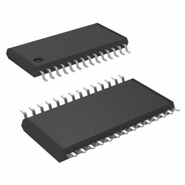
5T905PGGI
Obsolete2.5V SINGLE DATA RATE 1:5 CLOCK BUFFER TERABUFFER™

5T905PGGI
Obsolete2.5V SINGLE DATA RATE 1:5 CLOCK BUFFER TERABUFFER™
Description
General part information
5T905 Series
The 5T905 2.5V single data rate (SDR) clock buffer is a user-selectable single-ended or differential input to five single-ended outputs buffer built on advanced metal CMOS technology. The SDR clock buffer fanout from a single or differential input to five single-ended outputs reduces the loading on the preceding driver and provides an efficient clock distribution network. The 5T905 can act as a translator from a differential HSTL, eHSTL, 1.8V/2.5V LVTTL, LVEPECL, or single-ended 1.8V/2.5V LVTTL input to HSTL, eHSTL, 1.8V/2.5V LVTTL outputs. Selectable interface is controlled by 3-level input signals that may be hard-wired to appropriate high-mid-low levels. Multiple power and grounds reduce noise.
Technical Specifications
Parameters and characteristics for this part
| Specification | 5T905PGGI |
|---|---|
| Differential Input | Yes |
| Differential Output | No |
| Frequency - Max | 250 MHz |
| Input | eHSTL, LVTTL, LVPECL, HSTL |
| Input Ratio | 1 |
| Mounting Type | Surface Mount |
| Number of Circuits | 1 |
| Operating Temperature (Max) | 85 °C |
| Operating Temperature (Min) | -40 °C |
| Output | HSTL, EHSTL, LVTTL |
| Output Ratio | 5 |
| Package Length | 0.173 in |
| Package Name | 28-TSSOP |
| Package Width | 4.4 mm |
| Type | Fanout Buffer (Distribution) |
| Voltage - Supply (Maximum) | 2.6 V |
| Voltage - Supply (Minimum) | 2.4 V |
Pricing
Prices provided here are for design reference only. For realtime values and availability, please visit the distributors directly
Sign in to see pricing
Create a free account to access distributor pricing data.
CAD
3D models and CAD resources for this part
Documents
Technical documentation and resources