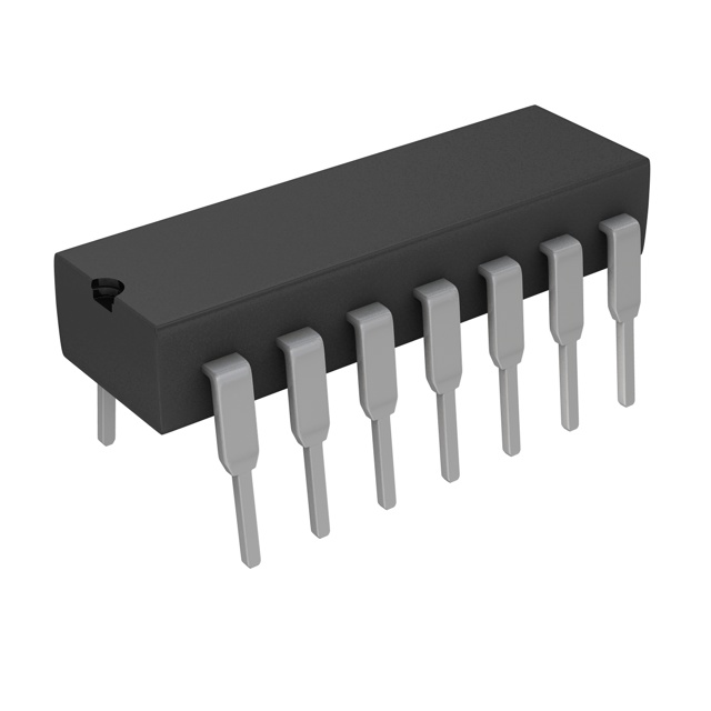
TPS3513N
Active3-CHANNEL SUPERVISOR WITH OVERCURRENT DETECT FOR SWITCH-MODE POWER SUPPLIES
Deep-Dive with AI
Search across all available documentation for this part.

TPS3513N
Active3-CHANNEL SUPERVISOR WITH OVERCURRENT DETECT FOR SWITCH-MODE POWER SUPPLIES
Deep-Dive with AI
Technical Specifications
Parameters and characteristics commom to parts in this series
| Specification | TPS3513N | TPS3513 Series |
|---|---|---|
| Mounting Type | Through Hole | Surface Mount, Through Hole |
| Number of Voltages Monitored | 3 | 3 |
| Operating Temperature [Max] | 85 °C | 85 °C |
| Operating Temperature [Min] | -40 °C | -40 °C |
| Output | Open Drain or Open Collector | Open Drain or Open Collector |
| Package / Case | 14-DIP | 14-SOIC, 14-DIP |
| Package / Case | 7.62 mm | 3.9 - 7.62 mm |
| Package / Case | 0.3 in | 0.154 - 0.3 in |
| Reset | Active Low | Active Low |
| Reset Timeout [Min] | 200 ms | 200 ms |
| Type | Multi-Voltage Supervisor | Multi-Voltage Supervisor |
| Voltage - Threshold | 12 V, 3.3 V, 5 V | 3.3 - 12 V |
Pricing
Prices provided here are for design reference only. For realtime values and availability, please visit the distributors directly
TPS3513 Series
3-channel supervisor with overcurrent detect for switch-mode power supplies
| Part | Number of Voltages Monitored | Output | Operating Temperature [Max] | Operating Temperature [Min] | Voltage - Threshold | Reset | Reset Timeout [Min] | Type | Package / Case | Package / Case | Package / Case | Mounting Type |
|---|---|---|---|---|---|---|---|---|---|---|---|---|
Texas Instruments TPS3513DRThe TPS3513 is designed to optimize PC switching power supply system with minimum external components. It provides undervoltage lockout (UVLO), protection circuits, power good indicator, and on/off control.
UVLO thresholds are 4.45 V (on) and 3.65 V (off). Overcurrent protection (OCP) and overvoltage protection (OVP) monitor 3.3 V, 5 V, and 12 V. When an OC or OV condition is detected, the power-good output (PGO) is asserted low and the fault protection output (FPO) is latched high.PSONfrom low-to-high resets the latch. The OCP function will be enabled 75 ms afterPSONgoes low, and a debounce of typically 38 ms. A built-in 2.3-ms delay with 38-ms debounce fromPSONtoFPOoutput is enabled at turnoff.
An external resistor is connected between the RI pin and the GND pin. This will introduce an accurate I(ref)for OCP function. The I(ref)range is from 12.5 µA to 62.5 µA. The formula for choosing RI resistor is V(RI)/I(ref). Three OCP comparators and the I(ref)section are supplied by VS12. The current draw from the VS12 pin is less than 1 mA.
The power good feature monitors PGI, 3.3 V and 5 V, and issues a power good signal when the output is ready.
The TPS3513 is characterized for operation from –40°C to 85°C.
The TPS3513 is designed to optimize PC switching power supply system with minimum external components. It provides undervoltage lockout (UVLO), protection circuits, power good indicator, and on/off control.
UVLO thresholds are 4.45 V (on) and 3.65 V (off). Overcurrent protection (OCP) and overvoltage protection (OVP) monitor 3.3 V, 5 V, and 12 V. When an OC or OV condition is detected, the power-good output (PGO) is asserted low and the fault protection output (FPO) is latched high.PSONfrom low-to-high resets the latch. The OCP function will be enabled 75 ms afterPSONgoes low, and a debounce of typically 38 ms. A built-in 2.3-ms delay with 38-ms debounce fromPSONtoFPOoutput is enabled at turnoff.
An external resistor is connected between the RI pin and the GND pin. This will introduce an accurate I(ref)for OCP function. The I(ref)range is from 12.5 µA to 62.5 µA. The formula for choosing RI resistor is V(RI)/I(ref). Three OCP comparators and the I(ref)section are supplied by VS12. The current draw from the VS12 pin is less than 1 mA.
The power good feature monitors PGI, 3.3 V and 5 V, and issues a power good signal when the output is ready.
The TPS3513 is characterized for operation from –40°C to 85°C. | 3 | Open Drain or Open Collector | 85 °C | -40 °C | 3.3 V, 5 V, 12 V | Active Low | 200 ms | Multi-Voltage Supervisor | 3.9 mm | 0.154 in | 14-SOIC | Surface Mount |
Texas Instruments TPS3513NThe TPS3513 is designed to optimize PC switching power supply system with minimum external components. It provides undervoltage lockout (UVLO), protection circuits, power good indicator, and on/off control.
UVLO thresholds are 4.45 V (on) and 3.65 V (off). Overcurrent protection (OCP) and overvoltage protection (OVP) monitor 3.3 V, 5 V, and 12 V. When an OC or OV condition is detected, the power-good output (PGO) is asserted low and the fault protection output (FPO) is latched high.PSONfrom low-to-high resets the latch. The OCP function will be enabled 75 ms afterPSONgoes low, and a debounce of typically 38 ms. A built-in 2.3-ms delay with 38-ms debounce fromPSONtoFPOoutput is enabled at turnoff.
An external resistor is connected between the RI pin and the GND pin. This will introduce an accurate I(ref)for OCP function. The I(ref)range is from 12.5 µA to 62.5 µA. The formula for choosing RI resistor is V(RI)/I(ref). Three OCP comparators and the I(ref)section are supplied by VS12. The current draw from the VS12 pin is less than 1 mA.
The power good feature monitors PGI, 3.3 V and 5 V, and issues a power good signal when the output is ready.
The TPS3513 is characterized for operation from –40°C to 85°C.
The TPS3513 is designed to optimize PC switching power supply system with minimum external components. It provides undervoltage lockout (UVLO), protection circuits, power good indicator, and on/off control.
UVLO thresholds are 4.45 V (on) and 3.65 V (off). Overcurrent protection (OCP) and overvoltage protection (OVP) monitor 3.3 V, 5 V, and 12 V. When an OC or OV condition is detected, the power-good output (PGO) is asserted low and the fault protection output (FPO) is latched high.PSONfrom low-to-high resets the latch. The OCP function will be enabled 75 ms afterPSONgoes low, and a debounce of typically 38 ms. A built-in 2.3-ms delay with 38-ms debounce fromPSONtoFPOoutput is enabled at turnoff.
An external resistor is connected between the RI pin and the GND pin. This will introduce an accurate I(ref)for OCP function. The I(ref)range is from 12.5 µA to 62.5 µA. The formula for choosing RI resistor is V(RI)/I(ref). Three OCP comparators and the I(ref)section are supplied by VS12. The current draw from the VS12 pin is less than 1 mA.
The power good feature monitors PGI, 3.3 V and 5 V, and issues a power good signal when the output is ready.
The TPS3513 is characterized for operation from –40°C to 85°C. | 3 | Open Drain or Open Collector | 85 °C | -40 °C | 3.3 V, 5 V, 12 V | Active Low | 200 ms | Multi-Voltage Supervisor | 7.62 mm | 0.3 in | 14-DIP | Through Hole |
Texas Instruments TPS3513DThe TPS3513 is designed to optimize PC switching power supply system with minimum external components. It provides undervoltage lockout (UVLO), protection circuits, power good indicator, and on/off control.
UVLO thresholds are 4.45 V (on) and 3.65 V (off). Overcurrent protection (OCP) and overvoltage protection (OVP) monitor 3.3 V, 5 V, and 12 V. When an OC or OV condition is detected, the power-good output (PGO) is asserted low and the fault protection output (FPO) is latched high.PSONfrom low-to-high resets the latch. The OCP function will be enabled 75 ms afterPSONgoes low, and a debounce of typically 38 ms. A built-in 2.3-ms delay with 38-ms debounce fromPSONtoFPOoutput is enabled at turnoff.
An external resistor is connected between the RI pin and the GND pin. This will introduce an accurate I(ref)for OCP function. The I(ref)range is from 12.5 µA to 62.5 µA. The formula for choosing RI resistor is V(RI)/I(ref). Three OCP comparators and the I(ref)section are supplied by VS12. The current draw from the VS12 pin is less than 1 mA.
The power good feature monitors PGI, 3.3 V and 5 V, and issues a power good signal when the output is ready.
The TPS3513 is characterized for operation from –40°C to 85°C.
The TPS3513 is designed to optimize PC switching power supply system with minimum external components. It provides undervoltage lockout (UVLO), protection circuits, power good indicator, and on/off control.
UVLO thresholds are 4.45 V (on) and 3.65 V (off). Overcurrent protection (OCP) and overvoltage protection (OVP) monitor 3.3 V, 5 V, and 12 V. When an OC or OV condition is detected, the power-good output (PGO) is asserted low and the fault protection output (FPO) is latched high.PSONfrom low-to-high resets the latch. The OCP function will be enabled 75 ms afterPSONgoes low, and a debounce of typically 38 ms. A built-in 2.3-ms delay with 38-ms debounce fromPSONtoFPOoutput is enabled at turnoff.
An external resistor is connected between the RI pin and the GND pin. This will introduce an accurate I(ref)for OCP function. The I(ref)range is from 12.5 µA to 62.5 µA. The formula for choosing RI resistor is V(RI)/I(ref). Three OCP comparators and the I(ref)section are supplied by VS12. The current draw from the VS12 pin is less than 1 mA.
The power good feature monitors PGI, 3.3 V and 5 V, and issues a power good signal when the output is ready.
The TPS3513 is characterized for operation from –40°C to 85°C. | 3 | Open Drain or Open Collector | 85 °C | -40 °C | 3.3 V, 5 V, 12 V | Active Low | 200 ms | Multi-Voltage Supervisor | 3.9 mm | 0.154 in | 14-SOIC | Surface Mount |
Description
General part information
TPS3513 Series
The TPS3513 is designed to optimize PC switching power supply system with minimum external components. It provides undervoltage lockout (UVLO), protection circuits, power good indicator, and on/off control.
UVLO thresholds are 4.45 V (on) and 3.65 V (off). Overcurrent protection (OCP) and overvoltage protection (OVP) monitor 3.3 V, 5 V, and 12 V. When an OC or OV condition is detected, the power-good output (PGO) is asserted low and the fault protection output (FPO) is latched high.PSONfrom low-to-high resets the latch. The OCP function will be enabled 75 ms afterPSONgoes low, and a debounce of typically 38 ms. A built-in 2.3-ms delay with 38-ms debounce fromPSONtoFPOoutput is enabled at turnoff.
An external resistor is connected between the RI pin and the GND pin. This will introduce an accurate I(ref)for OCP function. The I(ref)range is from 12.5 µA to 62.5 µA. The formula for choosing RI resistor is V(RI)/I(ref). Three OCP comparators and the I(ref)section are supplied by VS12. The current draw from the VS12 pin is less than 1 mA.
Documents
Technical documentation and resources


