CD54HC40103F
ActiveHIGH SPEED CMOS LOGIC 8-STAGE SYNCHRONOUS DOWN COUNTERS
Deep-Dive with AI
Search across all available documentation for this part.
CD54HC40103F
ActiveHIGH SPEED CMOS LOGIC 8-STAGE SYNCHRONOUS DOWN COUNTERS
Deep-Dive with AI
Technical Specifications
Parameters and characteristics commom to parts in this series
| Specification | CD54HC40103F | CD54HC40103 Series |
|---|---|---|
| Count Rate | 18 MHz | 18 MHz |
| Direction | Down | Down |
| Logic Type | Binary Counter | Binary Counter |
| Mounting Type | Through Hole | Through Hole |
| Number of Bits per Element | 8 | 8 |
| Number of Elements [custom] | 1 | 1 |
| Operating Temperature [Max] | 125 °C | 125 °C |
| Operating Temperature [Min] | -55 C | -55 C |
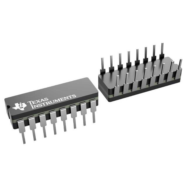
| Package / Case | 16-CDIP (0.300", 7.62mm) | 16-CDIP (0.300", 7.62mm) |
| Supplier Device Package | 16-CDIP | 16-CDIP |
| Timing | Synchronous | Synchronous |
| Trigger Type | Positive Edge | Positive Edge |
| Voltage - Supply [Max] | 6 V | 6 V |
| Voltage - Supply [Min] | 2 V | 2 V |
Pricing
Prices provided here are for design reference only. For realtime values and availability, please visit the distributors directly
CD54HC40103 Series
High Speed CMOS Logic 8-Stage Synchronous Down Counters
| Part | Operating Temperature [Min] | Operating Temperature [Max] | Number of Elements [custom] | Direction | Number of Bits per Element | Trigger Type | Package / Case | Supplier Device Package | Timing | Count Rate | Mounting Type | Voltage - Supply [Max] | Voltage - Supply [Min] | Logic Type |
|---|---|---|---|---|---|---|---|---|---|---|---|---|---|---|
Texas Instruments CD54HC40103FThe ’HC40103 and CD74HCT40103 are manufactured with high speed silicon gate technology and consist of an 8-stage synchronous down counter with a single output which is active when the internal count is zero. The 40103 contains a single 8-bit binary counter. Each has control inputs for enabling or disabling the clock, for clearing the counter to its maximum count, and for presetting the counter either synchronously or asynchronously. All control inputs and the TC\ output are active-low logic.
In normal operation, the counter is decremented by one count on each positive transition of the CLOCK (CP). Counting is inhibited when the TE\ input is high. The TC\ output goes low when the count reaches zero if the TE\ input is low, and remains low for one full clock period.
When the PE\ input is low, data at the P0-P7 inputs are clocked into the counter on the next positive clock transition regardless of the state of the TE\ input. When the PL\ input is low, data at the P0-P7 inputs are asynchronously forced into the counter regardless of the state of the PE\, TE\, or CLOCK inputs. Input P0-P7 represent a single 8-bit binary word for the 40103. When the MR input is low, the counter is asynchronously cleared to its maximum count of 25510, regardless of the state of any other input. The precedence relationship between control inputs is indicated in the truth table.
If all control inputs except TE\ are high at the time of zero count, the counters will jump to the maximum count, giving a counting sequence of 10016or 25610clock pulses long.
The 40103 may be cascaded using the TE\ input and the TC\ output, in either a synchronous or ripple mode. These circuits possess the low power consumption usually associated with CMOS circuitry, yet have speeds comparable to low power Schottky TTL circuits and can drive up to 10 LSTTL loads.
The ’HC40103 and CD74HCT40103 are manufactured with high speed silicon gate technology and consist of an 8-stage synchronous down counter with a single output which is active when the internal count is zero. The 40103 contains a single 8-bit binary counter. Each has control inputs for enabling or disabling the clock, for clearing the counter to its maximum count, and for presetting the counter either synchronously or asynchronously. All control inputs and the TC\ output are active-low logic.
In normal operation, the counter is decremented by one count on each positive transition of the CLOCK (CP). Counting is inhibited when the TE\ input is high. The TC\ output goes low when the count reaches zero if the TE\ input is low, and remains low for one full clock period.
When the PE\ input is low, data at the P0-P7 inputs are clocked into the counter on the next positive clock transition regardless of the state of the TE\ input. When the PL\ input is low, data at the P0-P7 inputs are asynchronously forced into the counter regardless of the state of the PE\, TE\, or CLOCK inputs. Input P0-P7 represent a single 8-bit binary word for the 40103. When the MR input is low, the counter is asynchronously cleared to its maximum count of 25510, regardless of the state of any other input. The precedence relationship between control inputs is indicated in the truth table.
If all control inputs except TE\ are high at the time of zero count, the counters will jump to the maximum count, giving a counting sequence of 10016or 25610clock pulses long.
The 40103 may be cascaded using the TE\ input and the TC\ output, in either a synchronous or ripple mode. These circuits possess the low power consumption usually associated with CMOS circuitry, yet have speeds comparable to low power Schottky TTL circuits and can drive up to 10 LSTTL loads. | -55 C | 125 °C | 1 | Down | 8 | Positive Edge | 16-CDIP (0.300", 7.62mm) | 16-CDIP | Synchronous | 18 MHz | Through Hole | 6 V | 2 V | Binary Counter |
Texas Instruments CD54HC40103F3AThe ’HC40103 and CD74HCT40103 are manufactured with high speed silicon gate technology and consist of an 8-stage synchronous down counter with a single output which is active when the internal count is zero. The 40103 contains a single 8-bit binary counter. Each has control inputs for enabling or disabling the clock, for clearing the counter to its maximum count, and for presetting the counter either synchronously or asynchronously. All control inputs and the TC\ output are active-low logic.
In normal operation, the counter is decremented by one count on each positive transition of the CLOCK (CP). Counting is inhibited when the TE\ input is high. The TC\ output goes low when the count reaches zero if the TE\ input is low, and remains low for one full clock period.
When the PE\ input is low, data at the P0-P7 inputs are clocked into the counter on the next positive clock transition regardless of the state of the TE\ input. When the PL\ input is low, data at the P0-P7 inputs are asynchronously forced into the counter regardless of the state of the PE\, TE\, or CLOCK inputs. Input P0-P7 represent a single 8-bit binary word for the 40103. When the MR input is low, the counter is asynchronously cleared to its maximum count of 25510, regardless of the state of any other input. The precedence relationship between control inputs is indicated in the truth table.
If all control inputs except TE\ are high at the time of zero count, the counters will jump to the maximum count, giving a counting sequence of 10016or 25610clock pulses long.
The 40103 may be cascaded using the TE\ input and the TC\ output, in either a synchronous or ripple mode. These circuits possess the low power consumption usually associated with CMOS circuitry, yet have speeds comparable to low power Schottky TTL circuits and can drive up to 10 LSTTL loads.
The ’HC40103 and CD74HCT40103 are manufactured with high speed silicon gate technology and consist of an 8-stage synchronous down counter with a single output which is active when the internal count is zero. The 40103 contains a single 8-bit binary counter. Each has control inputs for enabling or disabling the clock, for clearing the counter to its maximum count, and for presetting the counter either synchronously or asynchronously. All control inputs and the TC\ output are active-low logic.
In normal operation, the counter is decremented by one count on each positive transition of the CLOCK (CP). Counting is inhibited when the TE\ input is high. The TC\ output goes low when the count reaches zero if the TE\ input is low, and remains low for one full clock period.
When the PE\ input is low, data at the P0-P7 inputs are clocked into the counter on the next positive clock transition regardless of the state of the TE\ input. When the PL\ input is low, data at the P0-P7 inputs are asynchronously forced into the counter regardless of the state of the PE\, TE\, or CLOCK inputs. Input P0-P7 represent a single 8-bit binary word for the 40103. When the MR input is low, the counter is asynchronously cleared to its maximum count of 25510, regardless of the state of any other input. The precedence relationship between control inputs is indicated in the truth table.
If all control inputs except TE\ are high at the time of zero count, the counters will jump to the maximum count, giving a counting sequence of 10016or 25610clock pulses long.
The 40103 may be cascaded using the TE\ input and the TC\ output, in either a synchronous or ripple mode. These circuits possess the low power consumption usually associated with CMOS circuitry, yet have speeds comparable to low power Schottky TTL circuits and can drive up to 10 LSTTL loads. | -55 C | 125 °C | 1 | Down | 8 | Positive Edge | 16-CDIP (0.300", 7.62mm) | 16-CDIP | Synchronous | 18 MHz | Through Hole | 6 V | 2 V | Binary Counter |
Description
General part information
CD54HC40103 Series
The ’HC40103 and CD74HCT40103 are manufactured with high speed silicon gate technology and consist of an 8-stage synchronous down counter with a single output which is active when the internal count is zero. The 40103 contains a single 8-bit binary counter. Each has control inputs for enabling or disabling the clock, for clearing the counter to its maximum count, and for presetting the counter either synchronously or asynchronously. All control inputs and the TC\ output are active-low logic.
In normal operation, the counter is decremented by one count on each positive transition of the CLOCK (CP). Counting is inhibited when the TE\ input is high. The TC\ output goes low when the count reaches zero if the TE\ input is low, and remains low for one full clock period.
When the PE\ input is low, data at the P0-P7 inputs are clocked into the counter on the next positive clock transition regardless of the state of the TE\ input. When the PL\ input is low, data at the P0-P7 inputs are asynchronously forced into the counter regardless of the state of the PE\, TE\, or CLOCK inputs. Input P0-P7 represent a single 8-bit binary word for the 40103. When the MR input is low, the counter is asynchronously cleared to its maximum count of 25510, regardless of the state of any other input. The precedence relationship between control inputs is indicated in the truth table.
Documents
Technical documentation and resources