MPC9447AC
Obsolete3.3V,2.5V,1:9 LVCMOS CLOCK FANOUT BUFFER
MPC9447AC
Obsolete3.3V,2.5V,1:9 LVCMOS CLOCK FANOUT BUFFER
Description
General part information
MPC9447 Series
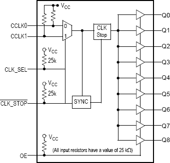
MPC9447 is specifically designed to distribute LVCMOS compatible clock signals up to a frequency of 350 MHz. Each output provides a precise copy of the input signal with a near zero skew. The outputs buffers support driving of 50 ? terminated transmission lines on the incident edge. Each is capable of driving either one parallel terminated or two series terminated transmission lines. Two selectable independent LVCMOS compatible clock inputs are available, providing support of redundant clock source systems. The MPC9447 CLK_STOP control is synchronous to the falling edge of the input clock. It allows the start and stop of the output clock signal only in a logic low state, and thus, eliminates potential output runt pulses. Applying the OE control will force the outputs into high-impedance mode. All inputs have an internal pull-up or pull-down resistor preventing unused and open inputs from floating. The device supports a 2.5 V or 3.3 V power supply and an ambient temperature range of -40°C to +85°C. The MPC9447 is pin and function compatible but performance-enhanced to the MPC947.
Technical Specifications
Parameters and characteristics for this part
| Specification | MPC9447AC |
|---|---|
| Differential Input | No |
| Differential Output | No |
| Frequency - Max | 350 MHz |
| Input | LVCMOS |
| Input Ratio | 2 |
| Mounting Type | Surface Mount |
| Number of Circuits | 1 |
| Operating Temperature (Max) | 85 °C |
| Operating Temperature (Min) | -40 °C |
| Output | LVCMOS |
| Output Ratio | 9 |
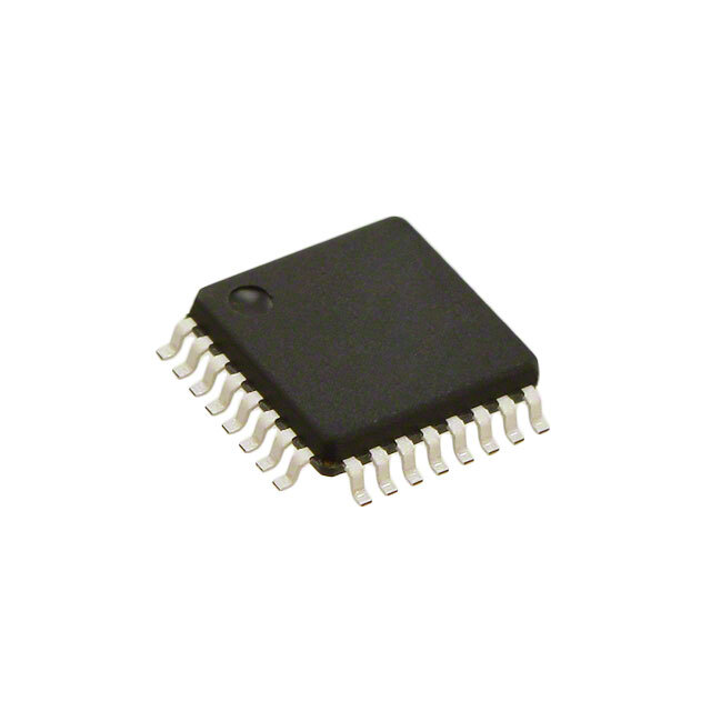
| Package / Case | 32-LQFP |
| Package Length | 7 mm |
| Package Name | 32-TQFP |
| Package Width | 7 mm |
| Type | Multiplexer, Fanout Buffer (Distribution) |
| Voltage - Supply (Maximum) | 3.465 V |
| Voltage - Supply (Minimum) | 2.375 V |
Pricing
Prices provided here are for design reference only. For realtime values and availability, please visit the distributors directly
Sign in to see pricing
Create a free account to access distributor pricing data.
CAD
3D models and CAD resources for this part
Documents
Technical documentation and resources