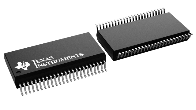
SN74LVC16T245DLR
Active16-BIT DUAL-SUPPLY BUS TRANSCEIVER WITH CONFIGURABLE LEVEL-SHIFTING / VOLTAGE TRANSLATION 48-SSOP -40 TO 85
Deep-Dive with AI
Search across all available documentation for this part.
SN74LVC16T245DLR
Active16-BIT DUAL-SUPPLY BUS TRANSCEIVER WITH CONFIGURABLE LEVEL-SHIFTING / VOLTAGE TRANSLATION 48-SSOP -40 TO 85
Technical Specifications
Parameters and characteristics commom to parts in this series
| Specification | SN74LVC16T245DLR | 74LVC16T245 Series |
|---|---|---|
| Current - Output High, Low [custom] | 32 mA | 32 mA |
| Current - Output High, Low [custom] | 32 mA | 32 mA |
| Logic Type | Translation Transceiver | Translation Transceiver |
| Mounting Type | Surface Mount | Surface Mount |
| Number of Bits per Element | 8 | 8 |
| Number of Elements [custom] | 2 | 2 |
| Operating Temperature [Max] | 85 °C | 85 °C |
| Operating Temperature [Min] | -40 °C | -40 °C |
| Output Type | 3-State | 3-State |
| Package / Case | 48-BSSOP (0.295", 7.50mm Width) | 56-VFBGA, 48-TFSOP, 48-BSSOP (0.295", 7.50mm Width) |
| Package / Case | - | 6.1 mm |
| Package / Case | - | 0.24 in |
| Supplier Device Package | 48-SSOP | 56-BGA Microstar Junior (7x4.5), 48-TSSOP, 48-SSOP |
| Voltage - Supply [Max] | 5.5 V | 5.5 V |
| Voltage - Supply [Min] | 1.65 V | 1.65 V |
Pricing
Prices provided here are for design reference only. For realtime values and availability, please visit the distributors directly
74LVC16T245 Series
16-bit dual-supply bus transceiver with configurable level-shifting / voltage translation
| Part | Voltage - Supply [Max] | Voltage - Supply [Min] | Package / Case | Output Type | Logic Type | Number of Bits per Element | Supplier Device Package | Number of Elements [custom] | Mounting Type | Current - Output High, Low [custom] | Current - Output High, Low [custom] | Operating Temperature [Max] | Operating Temperature [Min] | Package / Case [y] | Package / Case |
|---|---|---|---|---|---|---|---|---|---|---|---|---|---|---|---|
Texas Instruments SN74LVC16T245ZQLRTranslation Transceiver 2 Element 8 Bit per Element 3-State Output 56-BGA Microstar Junior (7x4.5) | 5.5 V | 1.65 V | 56-VFBGA | 3-State | Translation Transceiver | 8 | 56-BGA Microstar Junior (7x4.5) | 2 | Surface Mount | 32 mA | 32 mA | 85 °C | -40 °C | ||
Texas Instruments 74LVC16T245DGGRG4Translation Transceiver 2 Element 8 Bit per Element 3-State Output 48-TSSOP | 5.5 V | 1.65 V | 48-TFSOP | 3-State | Translation Transceiver | 8 | 48-TSSOP | 2 | Surface Mount | 32 mA | 32 mA | 85 °C | -40 °C | 6.1 mm | 0.24 in |
Texas Instruments SN74LVC16T245GQLRTranslation Transceiver 2 Element 8 Bit per Element 3-State Output 56-BGA Microstar Junior (7x4.5) | 5.5 V | 1.65 V | 56-VFBGA | 3-State | Translation Transceiver | 8 | 56-BGA Microstar Junior (7x4.5) | 2 | Surface Mount | 32 mA | 32 mA | 85 °C | -40 °C | ||
Texas Instruments CLVC16T245MDGGREPThis 16-bit noninverting bus transceiver uses two separate configurable power-supply rails. The A port is designed to track VCCA. VCCAaccepts any supply voltage from 1.65 V to 5.5 V. The B port is designed to track VCCB. VCCBaccepts any supply voltage from 1.65 V to 5.5 V. This allows for universal low-voltage bidirectional translation between any of the 1.8-V, 2.5-V, 3.3-V, and 5-V voltage nodes.
The SN74LVC16T245 is designed for asynchronous communication between two data buses. The logic levels of the direction-control (DIR) input and the output-enable (OE) input activate either the B-port outputs or the A-port outputs or place both output ports into the high-impedance mode. The device transmits data from the A bus to the B bus when the B-port outputs are activated, and from the B bus to the A bus when the A-port outputs are activated. The input circuitry on both A and B ports always is active and must have a logic HIGH or LOW level applied to prevent excess ICCand ICCZ.
The SN74LVC16T245 is designed so that the control pins (1DIR, 2DIR, 1OE, and 2OE) are supplied by VCCA.
This device is fully specified for partial-power-down applications using Ioff. The Ioffcircuitry disables the outputs, preventing damaging current backflow through the device when it is powered down.
The VCCisolation feature ensures that if either VCCinput is at GND, then both ports are in the high-impedance state.
To ensure the high-impedance state during power up or power down,OEshould be tied to VCCthrough a pullup resistor; the minimum value of the resistor is determined by the current-sinking capability of the driver.
This 16-bit noninverting bus transceiver uses two separate configurable power-supply rails. The A port is designed to track VCCA. VCCAaccepts any supply voltage from 1.65 V to 5.5 V. The B port is designed to track VCCB. VCCBaccepts any supply voltage from 1.65 V to 5.5 V. This allows for universal low-voltage bidirectional translation between any of the 1.8-V, 2.5-V, 3.3-V, and 5-V voltage nodes.
The SN74LVC16T245 is designed for asynchronous communication between two data buses. The logic levels of the direction-control (DIR) input and the output-enable (OE) input activate either the B-port outputs or the A-port outputs or place both output ports into the high-impedance mode. The device transmits data from the A bus to the B bus when the B-port outputs are activated, and from the B bus to the A bus when the A-port outputs are activated. The input circuitry on both A and B ports always is active and must have a logic HIGH or LOW level applied to prevent excess ICCand ICCZ.
The SN74LVC16T245 is designed so that the control pins (1DIR, 2DIR, 1OE, and 2OE) are supplied by VCCA.
This device is fully specified for partial-power-down applications using Ioff. The Ioffcircuitry disables the outputs, preventing damaging current backflow through the device when it is powered down.
The VCCisolation feature ensures that if either VCCinput is at GND, then both ports are in the high-impedance state.
To ensure the high-impedance state during power up or power down,OEshould be tied to VCCthrough a pullup resistor; the minimum value of the resistor is determined by the current-sinking capability of the driver. | 5.5 V | 1.65 V | 48-TFSOP | 3-State | Translation Transceiver | 8 | 48-TSSOP | 2 | Surface Mount | 32 mA | 32 mA | 85 °C | -40 °C | 6.1 mm | 0.24 in |
Texas Instruments SN74LVC16T245DGGRThis 16-bit noninverting bus transceiver uses two separate configurable power-supply rails. The A port is designed to track VCCA. VCCAaccepts any supply voltage from 1.65 V to 5.5 V. The B port is designed to track VCCB. VCCBaccepts any supply voltage from 1.65 V to 5.5 V. This allows for universal low-voltage bidirectional translation between any of the 1.8-V, 2.5-V, 3.3-V, and 5-V voltage nodes.
The SN74LVC16T245 device is designed for asynchronous communication between two data buses. The logic levels of the direction-control (DIR) input and the output-enable (OE) input activate either the B-port outputs or the A-port outputs or place both output ports into the high-impedance mode. The device transmits data from the A bus to the B bus when the B-port outputs are activated, and from the B bus to the A bus when the A-port outputs are activated. The input circuitry on both A and B ports always is active and must have a logic HIGH or LOW level applied to prevent excess ICCand ICCZ.
The SN74LVC16T245 control pins (1DIR, 2DIR, 1OE, and 2OE) are supplied by VCCA.
This device is fully specified for partial-power-down applications using Ioff. The Ioffcircuitry disables the outputs, preventing damaging current backflow through the device when it is powered down.
The VCCisolation feature ensures that if either VCCinput is at GND, then both ports are in the high-impedance state. To ensure the high-impedance state during power up or power down,OEshould be tied to VCCthrough a pullup resistor; the minimum value of the resistor is determined by the current-sinking capability of the driver.
This 16-bit noninverting bus transceiver uses two separate configurable power-supply rails. The A port is designed to track VCCA. VCCAaccepts any supply voltage from 1.65 V to 5.5 V. The B port is designed to track VCCB. VCCBaccepts any supply voltage from 1.65 V to 5.5 V. This allows for universal low-voltage bidirectional translation between any of the 1.8-V, 2.5-V, 3.3-V, and 5-V voltage nodes.
The SN74LVC16T245 device is designed for asynchronous communication between two data buses. The logic levels of the direction-control (DIR) input and the output-enable (OE) input activate either the B-port outputs or the A-port outputs or place both output ports into the high-impedance mode. The device transmits data from the A bus to the B bus when the B-port outputs are activated, and from the B bus to the A bus when the A-port outputs are activated. The input circuitry on both A and B ports always is active and must have a logic HIGH or LOW level applied to prevent excess ICCand ICCZ.
The SN74LVC16T245 control pins (1DIR, 2DIR, 1OE, and 2OE) are supplied by VCCA.
This device is fully specified for partial-power-down applications using Ioff. The Ioffcircuitry disables the outputs, preventing damaging current backflow through the device when it is powered down.
The VCCisolation feature ensures that if either VCCinput is at GND, then both ports are in the high-impedance state. To ensure the high-impedance state during power up or power down,OEshould be tied to VCCthrough a pullup resistor; the minimum value of the resistor is determined by the current-sinking capability of the driver. | 5.5 V | 1.65 V | 48-TFSOP | 3-State | Translation Transceiver | 8 | 48-TSSOP | 2 | Surface Mount | 32 mA | 32 mA | 85 °C | -40 °C | 6.1 mm | 0.24 in |
Texas Instruments CLVC16T245MDGGEPThis 16-bit noninverting bus transceiver uses two separate configurable power-supply rails. The A port is designed to track VCCA. VCCAaccepts any supply voltage from 1.65 V to 5.5 V. The B port is designed to track VCCB. VCCBaccepts any supply voltage from 1.65 V to 5.5 V. This allows for universal low-voltage bidirectional translation between any of the 1.8-V, 2.5-V, 3.3-V, and 5-V voltage nodes.
The SN74LVC16T245 is designed for asynchronous communication between two data buses. The logic levels of the direction-control (DIR) input and the output-enable (OE) input activate either the B-port outputs or the A-port outputs or place both output ports into the high-impedance mode. The device transmits data from the A bus to the B bus when the B-port outputs are activated, and from the B bus to the A bus when the A-port outputs are activated. The input circuitry on both A and B ports always is active and must have a logic HIGH or LOW level applied to prevent excess ICCand ICCZ.
The SN74LVC16T245 is designed so that the control pins (1DIR, 2DIR, 1OE, and 2OE) are supplied by VCCA.
This device is fully specified for partial-power-down applications using Ioff. The Ioffcircuitry disables the outputs, preventing damaging current backflow through the device when it is powered down.
The VCCisolation feature ensures that if either VCCinput is at GND, then both ports are in the high-impedance state.
To ensure the high-impedance state during power up or power down,OEshould be tied to VCCthrough a pullup resistor; the minimum value of the resistor is determined by the current-sinking capability of the driver.
This 16-bit noninverting bus transceiver uses two separate configurable power-supply rails. The A port is designed to track VCCA. VCCAaccepts any supply voltage from 1.65 V to 5.5 V. The B port is designed to track VCCB. VCCBaccepts any supply voltage from 1.65 V to 5.5 V. This allows for universal low-voltage bidirectional translation between any of the 1.8-V, 2.5-V, 3.3-V, and 5-V voltage nodes.
The SN74LVC16T245 is designed for asynchronous communication between two data buses. The logic levels of the direction-control (DIR) input and the output-enable (OE) input activate either the B-port outputs or the A-port outputs or place both output ports into the high-impedance mode. The device transmits data from the A bus to the B bus when the B-port outputs are activated, and from the B bus to the A bus when the A-port outputs are activated. The input circuitry on both A and B ports always is active and must have a logic HIGH or LOW level applied to prevent excess ICCand ICCZ.
The SN74LVC16T245 is designed so that the control pins (1DIR, 2DIR, 1OE, and 2OE) are supplied by VCCA.
This device is fully specified for partial-power-down applications using Ioff. The Ioffcircuitry disables the outputs, preventing damaging current backflow through the device when it is powered down.
The VCCisolation feature ensures that if either VCCinput is at GND, then both ports are in the high-impedance state.
To ensure the high-impedance state during power up or power down,OEshould be tied to VCCthrough a pullup resistor; the minimum value of the resistor is determined by the current-sinking capability of the driver. | 5.5 V | 1.65 V | 48-TFSOP | 3-State | Translation Transceiver | 8 | 48-TSSOP | 2 | Surface Mount | 32 mA | 32 mA | 85 °C | -40 °C | 6.1 mm | 0.24 in |
Texas Instruments SN74LVC16T245DLThis 16-bit noninverting bus transceiver uses two separate configurable power-supply rails. The A port is designed to track VCCA. VCCAaccepts any supply voltage from 1.65 V to 5.5 V. The B port is designed to track VCCB. VCCBaccepts any supply voltage from 1.65 V to 5.5 V. This allows for universal low-voltage bidirectional translation between any of the 1.8-V, 2.5-V, 3.3-V, and 5-V voltage nodes.
The SN74LVC16T245 device is designed for asynchronous communication between two data buses. The logic levels of the direction-control (DIR) input and the output-enable (OE) input activate either the B-port outputs or the A-port outputs or place both output ports into the high-impedance mode. The device transmits data from the A bus to the B bus when the B-port outputs are activated, and from the B bus to the A bus when the A-port outputs are activated. The input circuitry on both A and B ports always is active and must have a logic HIGH or LOW level applied to prevent excess ICCand ICCZ.
The SN74LVC16T245 control pins (1DIR, 2DIR, 1OE, and 2OE) are supplied by VCCA.
This device is fully specified for partial-power-down applications using Ioff. The Ioffcircuitry disables the outputs, preventing damaging current backflow through the device when it is powered down.
The VCCisolation feature ensures that if either VCCinput is at GND, then both ports are in the high-impedance state. To ensure the high-impedance state during power up or power down,OEshould be tied to VCCthrough a pullup resistor; the minimum value of the resistor is determined by the current-sinking capability of the driver.
This 16-bit noninverting bus transceiver uses two separate configurable power-supply rails. The A port is designed to track VCCA. VCCAaccepts any supply voltage from 1.65 V to 5.5 V. The B port is designed to track VCCB. VCCBaccepts any supply voltage from 1.65 V to 5.5 V. This allows for universal low-voltage bidirectional translation between any of the 1.8-V, 2.5-V, 3.3-V, and 5-V voltage nodes.
The SN74LVC16T245 device is designed for asynchronous communication between two data buses. The logic levels of the direction-control (DIR) input and the output-enable (OE) input activate either the B-port outputs or the A-port outputs or place both output ports into the high-impedance mode. The device transmits data from the A bus to the B bus when the B-port outputs are activated, and from the B bus to the A bus when the A-port outputs are activated. The input circuitry on both A and B ports always is active and must have a logic HIGH or LOW level applied to prevent excess ICCand ICCZ.
The SN74LVC16T245 control pins (1DIR, 2DIR, 1OE, and 2OE) are supplied by VCCA.
This device is fully specified for partial-power-down applications using Ioff. The Ioffcircuitry disables the outputs, preventing damaging current backflow through the device when it is powered down.
The VCCisolation feature ensures that if either VCCinput is at GND, then both ports are in the high-impedance state. To ensure the high-impedance state during power up or power down,OEshould be tied to VCCthrough a pullup resistor; the minimum value of the resistor is determined by the current-sinking capability of the driver. | 5.5 V | 1.65 V | 48-BSSOP (0.295", 7.50mm Width) | 3-State | Translation Transceiver | 8 | 48-SSOP | 2 | Surface Mount | 32 mA | 32 mA | 85 °C | -40 °C | ||
Texas Instruments 74LVC16T245DGGRE4Translation Transceiver 2 Element 8 Bit per Element 3-State Output 48-TSSOP | 5.5 V | 1.65 V | 48-TFSOP | 3-State | Translation Transceiver | 8 | 48-TSSOP | 2 | Surface Mount | 32 mA | 32 mA | 85 °C | -40 °C | 6.1 mm | 0.24 in |
Texas Instruments SN74LVC16T245DLRThis 16-bit noninverting bus transceiver uses two separate configurable power-supply rails. The A port is designed to track VCCA. VCCAaccepts any supply voltage from 1.65 V to 5.5 V. The B port is designed to track VCCB. VCCBaccepts any supply voltage from 1.65 V to 5.5 V. This allows for universal low-voltage bidirectional translation between any of the 1.8-V, 2.5-V, 3.3-V, and 5-V voltage nodes.
The SN74LVC16T245 device is designed for asynchronous communication between two data buses. The logic levels of the direction-control (DIR) input and the output-enable (OE) input activate either the B-port outputs or the A-port outputs or place both output ports into the high-impedance mode. The device transmits data from the A bus to the B bus when the B-port outputs are activated, and from the B bus to the A bus when the A-port outputs are activated. The input circuitry on both A and B ports always is active and must have a logic HIGH or LOW level applied to prevent excess ICCand ICCZ.
The SN74LVC16T245 control pins (1DIR, 2DIR, 1OE, and 2OE) are supplied by VCCA.
This device is fully specified for partial-power-down applications using Ioff. The Ioffcircuitry disables the outputs, preventing damaging current backflow through the device when it is powered down.
The VCCisolation feature ensures that if either VCCinput is at GND, then both ports are in the high-impedance state. To ensure the high-impedance state during power up or power down,OEshould be tied to VCCthrough a pullup resistor; the minimum value of the resistor is determined by the current-sinking capability of the driver.
This 16-bit noninverting bus transceiver uses two separate configurable power-supply rails. The A port is designed to track VCCA. VCCAaccepts any supply voltage from 1.65 V to 5.5 V. The B port is designed to track VCCB. VCCBaccepts any supply voltage from 1.65 V to 5.5 V. This allows for universal low-voltage bidirectional translation between any of the 1.8-V, 2.5-V, 3.3-V, and 5-V voltage nodes.
The SN74LVC16T245 device is designed for asynchronous communication between two data buses. The logic levels of the direction-control (DIR) input and the output-enable (OE) input activate either the B-port outputs or the A-port outputs or place both output ports into the high-impedance mode. The device transmits data from the A bus to the B bus when the B-port outputs are activated, and from the B bus to the A bus when the A-port outputs are activated. The input circuitry on both A and B ports always is active and must have a logic HIGH or LOW level applied to prevent excess ICCand ICCZ.
The SN74LVC16T245 control pins (1DIR, 2DIR, 1OE, and 2OE) are supplied by VCCA.
This device is fully specified for partial-power-down applications using Ioff. The Ioffcircuitry disables the outputs, preventing damaging current backflow through the device when it is powered down.
The VCCisolation feature ensures that if either VCCinput is at GND, then both ports are in the high-impedance state. To ensure the high-impedance state during power up or power down,OEshould be tied to VCCthrough a pullup resistor; the minimum value of the resistor is determined by the current-sinking capability of the driver. | 5.5 V | 1.65 V | 48-BSSOP (0.295", 7.50mm Width) | 3-State | Translation Transceiver | 8 | 48-SSOP | 2 | Surface Mount | 32 mA | 32 mA | 85 °C | -40 °C |
Description
General part information
74LVC16T245 Series
This 16-bit noninverting bus transceiver uses two separate configurable power-supply rails. The A port is designed to track VCCA. VCCAaccepts any supply voltage from 1.65 V to 5.5 V. The B port is designed to track VCCB. VCCBaccepts any supply voltage from 1.65 V to 5.5 V. This allows for universal low-voltage bidirectional translation between any of the 1.8-V, 2.5-V, 3.3-V, and 5-V voltage nodes.
The SN74LVC16T245 device is designed for asynchronous communication between two data buses. The logic levels of the direction-control (DIR) input and the output-enable (OE) input activate either the B-port outputs or the A-port outputs or place both output ports into the high-impedance mode. The device transmits data from the A bus to the B bus when the B-port outputs are activated, and from the B bus to the A bus when the A-port outputs are activated. The input circuitry on both A and B ports always is active and must have a logic HIGH or LOW level applied to prevent excess ICCand ICCZ.
The SN74LVC16T245 control pins (1DIR, 2DIR, 1OE, and 2OE) are supplied by VCCA.
Documents
Technical documentation and resources