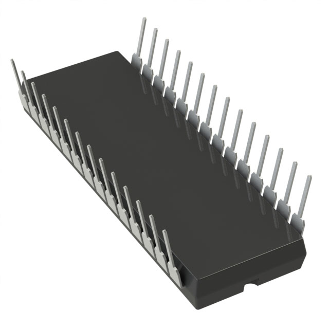
AD664JNZ-BIP
ActiveMONOLITHIC 12-BIT QUAD DAC
Deep-Dive with AI
Search across all available documentation for this part.

AD664JNZ-BIP
ActiveMONOLITHIC 12-BIT QUAD DAC
Deep-Dive with AI
Technical Specifications
Parameters and characteristics for this part
| Specification | AD664JNZ-BIP |
|---|---|
| Architecture | R-2R |
| Data Interface | Parallel |
| Differential Output | False |
| INL/DNL (LSB) | 0.75 LSB |
| INL/DNL (LSB) | ±0.75 (Max) |
| Mounting Type | Through Hole |
| Number of Bits | 12 bits |
| Number of D/A Converters | 4 |
| Operating Temperature [Max] | 70 °C |
| Operating Temperature [Min] | 0 °C |
| Output Type | Voltage - Buffered |
| Package / Case | 28-DIP |
| Package / Case | 0.6 in |
| Package / Case | 15.24 mm |
| Reference Type | External |
| Settling Time | 10 µs |
| Supplier Device Package | 28-PDIP |
| Voltage - Supply, Analog [Max] | 16.5 V |
| Voltage - Supply, Analog [Min] | -11.4 V |
| Voltage - Supply, Digital | 5 V |
Pricing
Prices provided here are for design reference only. For realtime values and availability, please visit the distributors directly
| Distributor | Package | Quantity | $ | |
|---|---|---|---|---|
| Digikey | Tube | 1 | $ 171.04 | |
| 10 | $ 141.76 | |||
| 25 | $ 139.01 | |||
Description
General part information
5962-8871902 Series
The AD664 is four complete 12-bit, voltage-output digital-toanalog converters (DACs) on one monolithic IC chip. Each DAC has a double buffered input latch structure and a data readback function. All DAC read and write operations occur through a single microprocessor-compatible input/output (I/O) port.The I/O port accommodates 4-bit, 8-bit, or 12-bit parallel words allowing simple interfacing with a wide variety of microprocessors. A reset to zero control pin is provided to allow a user to simultaneously reset all DAC outputs to zero, regardless of the contents of the input latch. Any one or all of the DACs may be placed in a transparent mode allowing immediate response by the outputs to the input data.The analog portion of the AD664 consists of four DAC cells, four output amplifiers, a control amplifier, and switches. Each DAC cell is an inverting R-2R type. The output current from each DAC is switched to the on-board application resistors and output amplifier. The output range of each DAC cell is programmed through the digital input/output port and may be set to unipolar (UNI) or bipolar (BIP) range, with a gain of one or two times the reference voltage. All DACs are operated from a single external referenceThe functional completeness of the AD664 results from the combination of the Analog Devices, Inc., BiMOS II process, laser trimmed thin film resistors, and double level metal interconnects.
Documents
Technical documentation and resources


