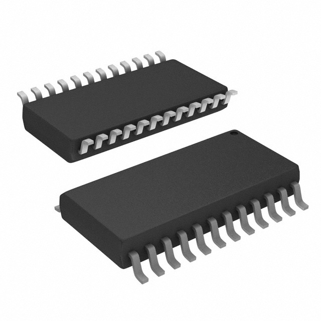
SN74LVC4245ADBR
ActiveOCTAL BUS TRANSCEIVER AND 3.3-V TO 5-V SHIFTER WITH 3-STATE OUTPUTS
SN74LVC4245ADBR
ActiveOCTAL BUS TRANSCEIVER AND 3.3-V TO 5-V SHIFTER WITH 3-STATE OUTPUTS
Description
General part information
74LVC4245 Series
This 8-bit (octal) noninverting bus transceiver contains two separate supply rails; B port has VCCB, which is set at 3.3 V, and A port has VCCA, which is set at 5 V. This allows for translation from a 3.3-V to a 5-V environment, and vice versa.
The SN74LVC4245A is designed for asynchronous communication between data buses. The device transmits data from the A bus to the B bus or from the B bus to the A bus, depending on the logic level at the direction-control (DIR) input. The output-enable (OE)\ input can be used to disable the device so the buses are effectively isolated.
The SN74LVC4245A pinout allows the designer to switch to a normal all-3.3-V or all-5-V 20-pin ’245 device without board re-layout. The designer uses the data paths for pins 2-11 and 14-23 of the SN74LVC4245A to align with the conventional ’245 pinout.
Technical Specifications
Parameters and characteristics for this part
| Specification | SN74LVC4245ADBR |
|---|---|
| Channel Type | Bidirectional |
| Channels per Circuit | 8 |
| Mounting Type | Surface Mount |
| Number of Circuits | 1 |
| Operating Temperature (Max) | 85 °C |
| Operating Temperature (Min) | -40 °C |
| Output Type | Tri-State |
| Package Length | 0.209 in |
| Package Name | 24-SSOP |
| Package Width | 5.3 mm |
| Translator Type | Voltage Level |
| Voltage - VCCA (Max) | 5.5 V |
| Voltage - VCCA (Min) | 4.5 V |
| Voltage - VCCB (Max) | 3.6 V |
| Voltage - VCCB (Min) | 2.7 V |
Pricing
Prices provided here are for design reference only. For realtime values and availability, please visit the distributors directly
Sign in to see pricing
Create a free account to access distributor pricing data.
CAD
3D models and CAD resources for this part
Documents
Technical documentation and resources