8V182512IDGGREP
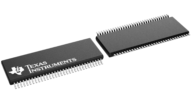
ActiveENHANCED PRODUCT 3.3-V ABT SCAN TEST DEVICES WITH 18-BIT UNIVERSAL BUS TRANSCEIVERS 64-TSSOP -40 TO 85
Deep-Dive with AI
Search across all available documentation for this part.
8V182512IDGGREP
ActiveENHANCED PRODUCT 3.3-V ABT SCAN TEST DEVICES WITH 18-BIT UNIVERSAL BUS TRANSCEIVERS 64-TSSOP -40 TO 85
Deep-Dive with AI
Technical Specifications
Parameters and characteristics commom to parts in this series
| Specification | 8V182512IDGGREP | SN74LVTH182512-EP Series |
|---|---|---|
| Logic Type | ABT Scan Test Device With Universal Bus Transceivers | ABT Scan Test Device With Universal Bus Transceivers |
| Mounting Type | Surface Mount | Surface Mount |
| Number of Bits | - | 9 |
| Operating Temperature [Max] | 85 °C | 85 °C |
| Operating Temperature [Min] | -40 °C | -40 °C |
| Package / Case | 0.24 in | 0.24 in |
| Package / Case | 64-TFSOP | 64-TFSOP |
| Package / Case [y] | 6.1 mm | 6.1 mm |
| Supplier Device Package | 64-TSSOP | 64-TSSOP |
| Supply Voltage [Max] | 3.6 V | 3.6 V |
| Supply Voltage [Min] | 2.7 VDC | 2.7 VDC |
Pricing
Prices provided here are for design reference only. For realtime values and availability, please visit the distributors directly
SN74LVTH182512-EP Series
Enhanced Product 3.3-V Abt Scan Test Devices With 18-Bit Universal Bus Transceivers
| Part | Package / Case | Package / Case | Package / Case [y] | Operating Temperature [Min] | Operating Temperature [Max] | Supply Voltage [Min] | Supply Voltage [Max] | Mounting Type | Supplier Device Package | Logic Type | Number of Bits |
|---|---|---|---|---|---|---|---|---|---|---|---|
Texas Instruments 8V182512IDGGREPThe SN74LVTH18512 and SN74LVTH182512 scan test devices with 18-bit universal bus transceivers are members of the Texas Instruments SCOPE™ testability integrated-circuit family. This family of devices supports IEEE Std 1149.1-1990 boundary scan to facilitate testing of complex circuit-board assemblies. Scan access to the test circuitry is accomplished via the 4-wire test access port (TAP) interface.
Additionally, these devices are designed specifically for low-voltage (3.3-V) VCCoperation, but with the capability to provide a TTL interface to a 5-V system environment.
In the normal mode, these devices are 18-bit universal bus transceivers that combine D-type latches and D-type flip-flops to allow data flow in transparent, latched, or clocked modes. They can be used either as two 9-bit transceivers or one 18-bit transceiver. The test circuitry can be activated by the TAP to take snapshot samples of the data appearing at the device pins or to perform a self test on the boundary-test cells. Activating the TAP in the normal mode does not affect the functional operation of the SCOPE™ universal bus transceivers.
Data flow in each direction is controlled by output-enable (OEAB\ and OEBA\), latch-enable (LEAB and LEBA), and clock (CLKAB and CLKBA) inputs. For A-to-B data flow, the devices operate in the transparent mode when LEAB is high. When LEAB is low, the A data is latched while CLKAB is held at a static low or high logic level. Otherwise, if LEAB is low, A data is stored on a low-to-high transition of CLKAB. When OEAB\ is low, the B outputs are active. When OEAB\ is high, the B outputs are in the high-impedance state. B-to-A data flow is similar to A-to-B data flow but uses the OEBA\, LEBA, and CLKBA inputs.
In the test mode, the normal operation of the SCOPE™ universal bus transceivers is inhibited, and the test circuitry is enabled to observe and control the I/O boundary of the device. When enabled, the test circuitry performs boundary-scan test operations according to the protocol described in IEEE Std 1149.1-1990.
Four dedicated test pins are used to observe and control the operation of the test circuitry: test data input (TDI), test data output (TDO), test mode select (TMS), and test clock (TCK). Additionally, the test circuitry performs other testing functions such as parallel-signature analysis (PSA) on data inputs and pseudo-random pattern generation (PRPG) from data outputs. All testing and scan operations are synchronized to the TAP interface.
Active bus-hold circuitry is provided to hold unused or floating data inputs at a valid logic level.
The B-port outputs of SN74LVTH182512, which are designed to source or sink up to 12 mA, include equivalent 25-series resistors to reduce overshoot and undershoot.
The SN74LVTH18512 and SN74LVTH182512 scan test devices with 18-bit universal bus transceivers are members of the Texas Instruments SCOPE™ testability integrated-circuit family. This family of devices supports IEEE Std 1149.1-1990 boundary scan to facilitate testing of complex circuit-board assemblies. Scan access to the test circuitry is accomplished via the 4-wire test access port (TAP) interface.
Additionally, these devices are designed specifically for low-voltage (3.3-V) VCCoperation, but with the capability to provide a TTL interface to a 5-V system environment.
In the normal mode, these devices are 18-bit universal bus transceivers that combine D-type latches and D-type flip-flops to allow data flow in transparent, latched, or clocked modes. They can be used either as two 9-bit transceivers or one 18-bit transceiver. The test circuitry can be activated by the TAP to take snapshot samples of the data appearing at the device pins or to perform a self test on the boundary-test cells. Activating the TAP in the normal mode does not affect the functional operation of the SCOPE™ universal bus transceivers.
Data flow in each direction is controlled by output-enable (OEAB\ and OEBA\), latch-enable (LEAB and LEBA), and clock (CLKAB and CLKBA) inputs. For A-to-B data flow, the devices operate in the transparent mode when LEAB is high. When LEAB is low, the A data is latched while CLKAB is held at a static low or high logic level. Otherwise, if LEAB is low, A data is stored on a low-to-high transition of CLKAB. When OEAB\ is low, the B outputs are active. When OEAB\ is high, the B outputs are in the high-impedance state. B-to-A data flow is similar to A-to-B data flow but uses the OEBA\, LEBA, and CLKBA inputs.
In the test mode, the normal operation of the SCOPE™ universal bus transceivers is inhibited, and the test circuitry is enabled to observe and control the I/O boundary of the device. When enabled, the test circuitry performs boundary-scan test operations according to the protocol described in IEEE Std 1149.1-1990.
Four dedicated test pins are used to observe and control the operation of the test circuitry: test data input (TDI), test data output (TDO), test mode select (TMS), and test clock (TCK). Additionally, the test circuitry performs other testing functions such as parallel-signature analysis (PSA) on data inputs and pseudo-random pattern generation (PRPG) from data outputs. All testing and scan operations are synchronized to the TAP interface.
Active bus-hold circuitry is provided to hold unused or floating data inputs at a valid logic level.
The B-port outputs of SN74LVTH182512, which are designed to source or sink up to 12 mA, include equivalent 25-series resistors to reduce overshoot and undershoot. | 0.24 in | 64-TFSOP | 6.1 mm | -40 °C | 85 °C | 2.7 VDC | 3.6 V | Surface Mount | 64-TSSOP | ABT Scan Test Device With Universal Bus Transceivers | |
Texas Instruments V62/04730-01XEThe SN74LVTH18512 and SN74LVTH182512 scan test devices with 18-bit universal bus transceivers are members of the Texas Instruments SCOPE™ testability integrated-circuit family. This family of devices supports IEEE Std 1149.1-1990 boundary scan to facilitate testing of complex circuit-board assemblies. Scan access to the test circuitry is accomplished via the 4-wire test access port (TAP) interface.
Additionally, these devices are designed specifically for low-voltage (3.3-V) VCCoperation, but with the capability to provide a TTL interface to a 5-V system environment.
In the normal mode, these devices are 18-bit universal bus transceivers that combine D-type latches and D-type flip-flops to allow data flow in transparent, latched, or clocked modes. They can be used either as two 9-bit transceivers or one 18-bit transceiver. The test circuitry can be activated by the TAP to take snapshot samples of the data appearing at the device pins or to perform a self test on the boundary-test cells. Activating the TAP in the normal mode does not affect the functional operation of the SCOPE™ universal bus transceivers.
Data flow in each direction is controlled by output-enable (OEAB\ and OEBA\), latch-enable (LEAB and LEBA), and clock (CLKAB and CLKBA) inputs. For A-to-B data flow, the devices operate in the transparent mode when LEAB is high. When LEAB is low, the A data is latched while CLKAB is held at a static low or high logic level. Otherwise, if LEAB is low, A data is stored on a low-to-high transition of CLKAB. When OEAB\ is low, the B outputs are active. When OEAB\ is high, the B outputs are in the high-impedance state. B-to-A data flow is similar to A-to-B data flow but uses the OEBA\, LEBA, and CLKBA inputs.
In the test mode, the normal operation of the SCOPE™ universal bus transceivers is inhibited, and the test circuitry is enabled to observe and control the I/O boundary of the device. When enabled, the test circuitry performs boundary-scan test operations according to the protocol described in IEEE Std 1149.1-1990.
Four dedicated test pins are used to observe and control the operation of the test circuitry: test data input (TDI), test data output (TDO), test mode select (TMS), and test clock (TCK). Additionally, the test circuitry performs other testing functions such as parallel-signature analysis (PSA) on data inputs and pseudo-random pattern generation (PRPG) from data outputs. All testing and scan operations are synchronized to the TAP interface.
Active bus-hold circuitry is provided to hold unused or floating data inputs at a valid logic level.
The B-port outputs of SN74LVTH182512, which are designed to source or sink up to 12 mA, include equivalent 25-series resistors to reduce overshoot and undershoot.
The SN74LVTH18512 and SN74LVTH182512 scan test devices with 18-bit universal bus transceivers are members of the Texas Instruments SCOPE™ testability integrated-circuit family. This family of devices supports IEEE Std 1149.1-1990 boundary scan to facilitate testing of complex circuit-board assemblies. Scan access to the test circuitry is accomplished via the 4-wire test access port (TAP) interface.
Additionally, these devices are designed specifically for low-voltage (3.3-V) VCCoperation, but with the capability to provide a TTL interface to a 5-V system environment.
In the normal mode, these devices are 18-bit universal bus transceivers that combine D-type latches and D-type flip-flops to allow data flow in transparent, latched, or clocked modes. They can be used either as two 9-bit transceivers or one 18-bit transceiver. The test circuitry can be activated by the TAP to take snapshot samples of the data appearing at the device pins or to perform a self test on the boundary-test cells. Activating the TAP in the normal mode does not affect the functional operation of the SCOPE™ universal bus transceivers.
Data flow in each direction is controlled by output-enable (OEAB\ and OEBA\), latch-enable (LEAB and LEBA), and clock (CLKAB and CLKBA) inputs. For A-to-B data flow, the devices operate in the transparent mode when LEAB is high. When LEAB is low, the A data is latched while CLKAB is held at a static low or high logic level. Otherwise, if LEAB is low, A data is stored on a low-to-high transition of CLKAB. When OEAB\ is low, the B outputs are active. When OEAB\ is high, the B outputs are in the high-impedance state. B-to-A data flow is similar to A-to-B data flow but uses the OEBA\, LEBA, and CLKBA inputs.
In the test mode, the normal operation of the SCOPE™ universal bus transceivers is inhibited, and the test circuitry is enabled to observe and control the I/O boundary of the device. When enabled, the test circuitry performs boundary-scan test operations according to the protocol described in IEEE Std 1149.1-1990.
Four dedicated test pins are used to observe and control the operation of the test circuitry: test data input (TDI), test data output (TDO), test mode select (TMS), and test clock (TCK). Additionally, the test circuitry performs other testing functions such as parallel-signature analysis (PSA) on data inputs and pseudo-random pattern generation (PRPG) from data outputs. All testing and scan operations are synchronized to the TAP interface.
Active bus-hold circuitry is provided to hold unused or floating data inputs at a valid logic level.
The B-port outputs of SN74LVTH182512, which are designed to source or sink up to 12 mA, include equivalent 25-series resistors to reduce overshoot and undershoot. | 0.24 in | 64-TFSOP | 6.1 mm | -40 °C | 85 °C | 2.7 VDC | 3.6 V | Surface Mount | 64-TSSOP | ABT Scan Test Device With Universal Bus Transceivers | 9 |
Description
General part information
SN74LVTH182512-EP Series
The SN74LVTH18512 and SN74LVTH182512 scan test devices with 18-bit universal bus transceivers are members of the Texas Instruments SCOPE™ testability integrated-circuit family. This family of devices supports IEEE Std 1149.1-1990 boundary scan to facilitate testing of complex circuit-board assemblies. Scan access to the test circuitry is accomplished via the 4-wire test access port (TAP) interface.
Additionally, these devices are designed specifically for low-voltage (3.3-V) VCCoperation, but with the capability to provide a TTL interface to a 5-V system environment.
In the normal mode, these devices are 18-bit universal bus transceivers that combine D-type latches and D-type flip-flops to allow data flow in transparent, latched, or clocked modes. They can be used either as two 9-bit transceivers or one 18-bit transceiver. The test circuitry can be activated by the TAP to take snapshot samples of the data appearing at the device pins or to perform a self test on the boundary-test cells. Activating the TAP in the normal mode does not affect the functional operation of the SCOPE™ universal bus transceivers.
Documents
Technical documentation and resources