9DB1233AGLF
Obsolete12-OUTPUT 3.3 V PCIE GEN1-2-3 ZERO DELAY / FANOUT BUFFER
9DB1233AGLF
Obsolete12-OUTPUT 3.3 V PCIE GEN1-2-3 ZERO DELAY / FANOUT BUFFER
Description
General part information
9DB1233 Series
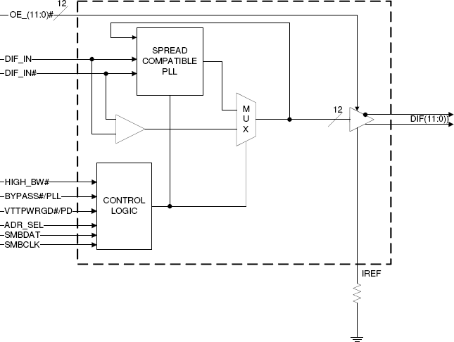
The 9DB1233 zero-delay buffer supports PCIe Gen3 requirements, while being backwards compatible to PCIe Gen2 and Gen1. The 9DB1233 is driven by a differential SRC output pair from an IDT 932S421 or 932SQ420 or equivalent main clock generator. It attenuates jitter on the input clock and has a selectable PLL bandwidth to maximize performance in systems with or without Spread-Spectrum clocking.
Technical Specifications
Parameters and characteristics for this part
| Specification | 9DB1233AGLF |
|---|---|
| Differential Input | Yes |
| Differential Output | Yes |
| Frequency - Max | 166 MHz |
| Input | Clock |
| Input Ratio | 1 |
| Main Purpose | PCI Express (PCIe) |
| Mounting Type | Surface Mount |
| Number of Circuits | 1 |
| Operating Temperature (Max) | 70 °C |
| Operating Temperature (Min) | 0 °C |
| Output | HCSL |
| Output Ratio | 12 |
| Package Length | 0.24 in |
| Package Name | 64-TFSOP, 64-TSSOP |
| Package Width | 6.1 mm |
| PLL | Yes |
| Voltage - Supply (Maximum) | 3.465 V |
| Voltage - Supply (Minimum) | 3.135 V |
Pricing
Prices provided here are for design reference only. For realtime values and availability, please visit the distributors directly
Sign in to see pricing
Create a free account to access distributor pricing data.
CAD
3D models and CAD resources for this part
Documents
Technical documentation and resources