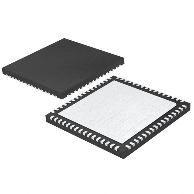
LTC2241CUP-10#TRPBF
ActiveIC ADC 10BIT PIPELINED 64QFN
Deep-Dive with AI
Search across all available documentation for this part.

LTC2241CUP-10#TRPBF
ActiveIC ADC 10BIT PIPELINED 64QFN
Deep-Dive with AI
Technical Specifications
Parameters and characteristics for this part
| Specification | LTC2241CUP-10#TRPBF |
|---|---|
| Architecture | Pipelined |
| Configuration | S/H-ADC |
| Data Interface | LVDS - Parallel, Parallel |
| Input Type | Differential |
| Mounting Type | Surface Mount |
| Number of A/D Converters | 1 |
| Number of Bits [custom] | 10 |
| Number of Inputs | 1 |
| Operating Temperature [Max] | 70 °C |
| Operating Temperature [Min] | 0 °C |
| Package / Case | 64-WFQFN Exposed Pad |
| Ratio - S/H:ADC | 1:1 |
| Reference Type | External, Internal |
| Sampling Rate (Per Second) | 210 M per second |
| Supplier Device Package | 64-QFN (9x9) |
| Voltage - Supply, Analog [Max] | 2.625 V |
| Voltage - Supply, Analog [Min] | 2.375 V |
| Voltage - Supply, Digital [Max] | 2.625 V |
| Voltage - Supply, Digital [Min] | 2.375 V |
Pricing
Prices provided here are for design reference only. For realtime values and availability, please visit the distributors directly
| Distributor | Package | Quantity | $ | |
|---|---|---|---|---|
| Digikey | Tape & Reel (TR) | 2000 | $ 47.23 | |
Description
General part information
LTC2241-12 Series
The LTC2241-10 is a 210Msps, sampling 10-bit A/D converter designed for digitizing high frequency, wide dynamic range signals. The LTC2241-10 is perfect for demanding communications applications with AC performance that includes 60.5dB SNR and 78dB SFDR. Ultralow jitter of 95fsRMSallows IF undersampling with excellent noise performance.DC specs include ±0.3LSB INL (typ), ±0.15LSB DNL (typ) and no missing codes over temperature.The digital outputs can be either differential LVDS, or single-ended CMOS. There are three format options for the CMOS outputs: a single bus running at the full data rate or two demultiplexed buses running at half data rate with either interleaved or simultaneous update. A separate output power supply allows the CMOS output swing to range from 0.5V to 2.625V.The ENC+and ENC–inputs may be driven differentially or single ended with a sine wave, PECL, LVDS, TTL, or CMOS inputs. An optional clock duty cycle stabilizer allows high performance over a wide range of clock duty cycles.BitsLTC2241-1010LTC2241-1212ApplicationsWireless and Wired Broadband CommunicationCable Head-End SystemsPower Amplifier LinearizationCommunications Test Equipment
Documents
Technical documentation and resources


