


859S0424BGILFT
Obsolete4:4 DIFFERENTIAL-TO-LVPECL/LVDS CLOCK MULTIPLEXER
859S0424BGILFT
Obsolete4:4 DIFFERENTIAL-TO-LVPECL/LVDS CLOCK MULTIPLEXER
Description
General part information
859S0424I Series
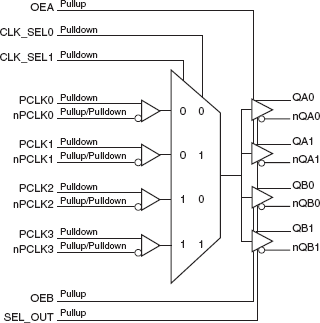
The 859S0424I is a 4:4 Differential-to-LVPECL/ LVDS Clock Multiplexer which can operate up to 3GHz. The outputs for this device can either be programmed to give LVPECL or LVDS levels. The 859S0424I has four selectable differential PCLKx, nPCLKx clock inputs. The PCLKx, nPCLKx input pairs can accept LVPECL, LVDS or CML levels. The fully differential architecture and low propagation delay make it ideal for use in clock distribution circuits.
Technical Specifications
Parameters and characteristics for this part
| Specification | 859S0424BGILFT |
|---|---|
| Differential Input | Yes |
| Differential Output | Yes |
| Frequency - Max | 3 GHz |
| Input | LVDS, CML, LVPECL |
| Input Ratio | 4 |
| Mounting Type | Surface Mount |
| Number of Circuits | 1 |
| Operating Temperature (Max) | 85 °C |
| Operating Temperature (Min) | -40 °C |
| Output | LVPECL, CML, LVDS |
| Output Ratio | 4 |
| Package Length | 0.173 in |
| Package Name | 24-TSSOP |
| Package Width | 4.4 mm |
| Type | Multiplexer, Fanout Buffer (Distribution) |
| Voltage - Supply (Range 1 Maximum) | 2.625 V |
| Voltage - Supply (Range 1 Minimum) | 2.375 V |
| Voltage - Supply (Range 2 Maximum) | 3.465 V |
| Voltage - Supply (Range 2 Minimum) | 3.135 V |
Pricing
Prices provided here are for design reference only. For realtime values and availability, please visit the distributors directly
Sign in to see pricing
Create a free account to access distributor pricing data.
CAD
3D models and CAD resources for this part
Documents
Technical documentation and resources

