TPS71257DRCR
Active250-MA, DUAL-CHANNEL LOW-DROPOUT VOLTAGE REGULATOR WITH ENABLE
TPS71257DRCR
Active250-MA, DUAL-CHANNEL LOW-DROPOUT VOLTAGE REGULATOR WITH ENABLE
Description
General part information
TPS712 Series
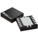
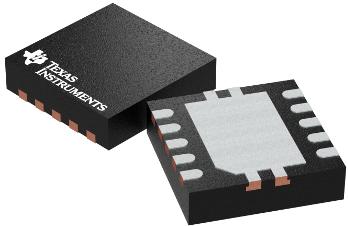
The TPS712xx family of low-dropout (LDO) voltage regulators is tailored to noise-sensitive and RF applications. These products feature dual 250 mA LDOs with ultralow noise, high power-supply rejection ratio (PSRR), and fast transient and start-up response. Each regulator output is stable with low-cost 2.2 µF ceramic output capacitors and features very low dropout voltages (125 mV typical at 250 mA). Each regulator achieves fast start-up times (approximately 60 µs with a 0.001 µF bypass capacitor) while consuming very low quiescent current (300 µA typical with both outputs enabled). When the device is placed in standby mode, the supply current is reduced to less than 0.3 µA typical. Each regulator exhibits approximately 32 µrms of output voltage noise with VOUT= 2.8 V and a 0.01 µF noise reduction (NR) capacitor. Applications with analog components that are noise-sensitive, such as portable RF electronics, will benefit from high PSRR, low noise, and fast line and load transient features. The TPS712 family is offered in a thin 3mm × 3mm SON package and is fully specified from –40°C to +125°C (TJ).
The TPS712xx family of low-dropout (LDO) voltage regulators is tailored to noise-sensitive and RF applications. These products feature dual 250 mA LDOs with ultralow noise, high power-supply rejection ratio (PSRR), and fast transient and start-up response. Each regulator output is stable with low-cost 2.2 µF ceramic output capacitors and features very low dropout voltages (125 mV typical at 250 mA). Each regulator achieves fast start-up times (approximately 60 µs with a 0.001 µF bypass capacitor) while consuming very low quiescent current (300 µA typical with both outputs enabled). When the device is placed in standby mode, the supply current is reduced to less than 0.3 µA typical. Each regulator exhibits approximately 32 µrms of output voltage noise with VOUT= 2.8 V and a 0.01 µF noise reduction (NR) capacitor. Applications with analog components that are noise-sensitive, such as portable RF electronics, will benefit from high PSRR, low noise, and fast line and load transient features. The TPS712 family is offered in a thin 3mm × 3mm SON package and is fully specified from –40°C to +125°C (TJ).
Technical Specifications
Parameters and characteristics for this part
| Specification | TPS71257DRCR |
|---|---|
| Control Features | Power Good, Enable |
| Current - Output | 250 mA |
| Current - Quiescent (Iq) | 250 µA |
| Current - Supply (Max) | 600 µA |
| Mounting Type | Surface Mount |
| Number of Regulators | 2 |
| Operating Temperature (Max) | 125 °C |
| Operating Temperature (Min) | -40 °C |
| Output Configuration | Positive |
| Output Type | Fixed |
| Package / Case | 10-VFDFN Exposed Pad |
| Package Length | 3 mm |
| Package Name | 10-VSON |
| Package Width | 3 mm |
| Protection Features | Under Voltage Lockout (UVLO), Reverse Polarity, Over Temperature |
| PSRR (Maximum) | 59 dB |
| PSRR (Minimum) | 54 dB |
| Voltage - Input (Max) | 5.5 V |
| Voltage - Output (Min/Fixed) | 2.85 V |
| Voltage Dropout (Max) | 0.4 V |
Pricing
Prices provided here are for design reference only. For realtime values and availability, please visit the distributors directly
Sign in to see pricing
Create a free account to access distributor pricing data.
CAD
3D models and CAD resources for this part
Documents
Technical documentation and resources