


72V2103L7-5BC
Obsolete128K X 18 / 256K X 9 SUPERSYNC II FIFO, 3.3V
72V2103L7-5BC
Obsolete128K X 18 / 256K X 9 SUPERSYNC II FIFO, 3.3V
Description
General part information
72V2103 Series
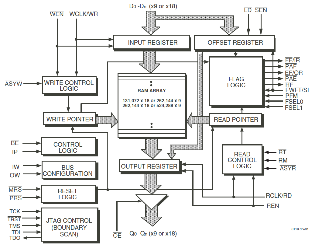
The 72V2103 256K x 9/128K x 18 SuperSync II FIFO memory has flexible x9/x18 Bus-Matching on both read and write ports. The variable clock cycle counting delay associated with the latency period found on previous SuperSync devices has been eliminated. SuperSync II FIFOs are appropriate for network, video, telecommunications, data communications and other applications that need to buffer large amounts of data and match buses of unequal sizes.
Technical Specifications
Parameters and characteristics for this part
| Specification | 72V2103L7-5BC |
|---|---|
| Access Time | 5 ns |
| Bus Directional | Uni-Directional |
| Current - Supply (Max) | 35 mA |
| Data Rate | 133.3 MHz |
| Expansion Type | Width, Depth |
| Function | Synchronous |
| FWFT Support | Yes |
| Memory Depth | 128 K |
| Memory Depth (Variant 2) | 256 K |
| Memory Size (Total) | 2.25 M |
| Memory Width | 18 bit |
| Memory Width (Variant 2) | 9 bit |
| Mounting Type | Surface Mount |
| Operating Temperature (Max) | 70 °C |
| Operating Temperature (Min) | 0 °C |
| Package / Case | 100-LBGA |
| Package Length | 11 mm |
| Package Name | 100-CABGA |
| Package Width | 11 mm |
| Programmable Flags Support | Yes |
| Retransmit Capability | Yes |
| Voltage - Supply (Maximum) | 3.45 V |
| Voltage - Supply (Minimum) | 3.15 V |
Pricing
Prices provided here are for design reference only. For realtime values and availability, please visit the distributors directly
Sign in to see pricing
Create a free account to access distributor pricing data.
CAD
3D models and CAD resources for this part
Documents
Technical documentation and resources


