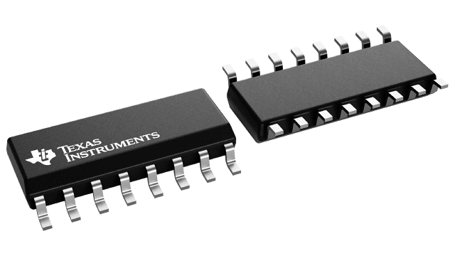
SN74LVC138AQDRQ1
ActiveAUTOMOTIVE CATALOG 3-LINE TO 8-LINE DECODER/DEMULTIPLEXER
Deep-Dive with AI
Search across all available documentation for this part.

SN74LVC138AQDRQ1
ActiveAUTOMOTIVE CATALOG 3-LINE TO 8-LINE DECODER/DEMULTIPLEXER
Technical Specifications
Parameters and characteristics commom to parts in this series
| Specification | SN74LVC138AQDRQ1 | SN74LVC138A-Q1 Series |
|---|---|---|
| Circuit | 1 x 3:8 | 1 x 3:8 |
| Current - Output High, Low [custom] | 24 mA | 24 mA |
| Current - Output High, Low [custom] | 24 mA | 24 mA |
| Grade | Automotive | Automotive |
| Independent Circuits | 1 | 1 |
| Mounting Type | Surface Mount | Surface Mount |
| Operating Temperature [Max] | 125 °C | 125 °C |
| Operating Temperature [Min] | -40 °C | -40 °C |
| Package / Case | 16-SOIC | 16-TSSOP, 16-SOIC |
| Package / Case | 3.9 mm Width, 0.154 in | 0.154 - 3.9 mm Width |
| Package / Case | - | 0.173 " |
| Package / Case | - | 4.4 mm |
| Qualification | AEC-Q100 | AEC-Q100 |
| Supplier Device Package | 16-SOIC | 16-TSSOP, 16-SOIC |
| Type | Decoder/Demultiplexer | Decoder/Demultiplexer |
| Voltage - Supply [Max] | 3.6 V | 3.6 V |
| Voltage - Supply [Min] | 2 V | 2 V |
| Voltage Supply Source | Single Supply | Single Supply |
Pricing
Prices provided here are for design reference only. For realtime values and availability, please visit the distributors directly
SN74LVC138A-Q1 Series
Automotive Catalog 3-Line To 8-Line decoder/Demultiplexer
| Part | Current - Output High, Low [custom] | Current - Output High, Low [custom] | Operating Temperature [Max] | Operating Temperature [Min] | Independent Circuits | Mounting Type | Circuit | Grade | Type | Voltage Supply Source | Supplier Device Package | Voltage - Supply [Max] | Voltage - Supply [Min] | Qualification | Package / Case [x] | Package / Case | Package / Case [x] | Package / Case |
|---|---|---|---|---|---|---|---|---|---|---|---|---|---|---|---|---|---|---|
Texas Instruments CLVC138AQPWRG4Q1The SN74LVC138A 3-line to 8-line decoder/demultiplexer is designed for 2.7-V to 3.6-V VCC operation.
The device is designed for high-performance memory-decoding or data-routing applications requiring very short propagation delay times. In high-performance memory systems, this decoder minimizes the effects of system decoding. When employed with high-speed memories utilizing a fast enable circuit, delay times of this decoder and the enable time of the memory usually are less than the typical access time of the memory. This means that the effective system delay introduced by the decoder is negligible.
The conditions at the binary-select inputs and the three enable inputs select one of eight output lines. Two active-low enable inputs and one active-high enable input reduce the need for external gates or inverters when expanding. A 24-line decoder can be implemented without external inverters, and a 32-line decoder requires only one inverter. An enable input can be used as a data input for demultiplexing applications.
Inputs can be driven from either 3.3-V or 5-V devices. This feature allows the use of this device as a translator in a mixed 3.3-V/5-V system environment.
The SN74LVC138A 3-line to 8-line decoder/demultiplexer is designed for 2.7-V to 3.6-V VCC operation.
The device is designed for high-performance memory-decoding or data-routing applications requiring very short propagation delay times. In high-performance memory systems, this decoder minimizes the effects of system decoding. When employed with high-speed memories utilizing a fast enable circuit, delay times of this decoder and the enable time of the memory usually are less than the typical access time of the memory. This means that the effective system delay introduced by the decoder is negligible.
The conditions at the binary-select inputs and the three enable inputs select one of eight output lines. Two active-low enable inputs and one active-high enable input reduce the need for external gates or inverters when expanding. A 24-line decoder can be implemented without external inverters, and a 32-line decoder requires only one inverter. An enable input can be used as a data input for demultiplexing applications.
Inputs can be driven from either 3.3-V or 5-V devices. This feature allows the use of this device as a translator in a mixed 3.3-V/5-V system environment. | 24 mA | 24 mA | 125 °C | -40 °C | 1 | Surface Mount | 1 x 3:8 | Automotive | Decoder/Demultiplexer | Single Supply | 16-TSSOP | 3.6 V | 2 V | AEC-Q100 | 0.173 " | 16-TSSOP | 4.4 mm | |
Texas Instruments SN74LVC138AQDRQ1The SN74LVC138A 3-line to 8-line decoder/demultiplexer is designed for 2.7-V to 3.6-V VCC operation.
The device is designed for high-performance memory-decoding or data-routing applications requiring very short propagation delay times. In high-performance memory systems, this decoder minimizes the effects of system decoding. When employed with high-speed memories utilizing a fast enable circuit, delay times of this decoder and the enable time of the memory usually are less than the typical access time of the memory. This means that the effective system delay introduced by the decoder is negligible.
The conditions at the binary-select inputs and the three enable inputs select one of eight output lines. Two active-low enable inputs and one active-high enable input reduce the need for external gates or inverters when expanding. A 24-line decoder can be implemented without external inverters, and a 32-line decoder requires only one inverter. An enable input can be used as a data input for demultiplexing applications.
Inputs can be driven from either 3.3-V or 5-V devices. This feature allows the use of this device as a translator in a mixed 3.3-V/5-V system environment.
The SN74LVC138A 3-line to 8-line decoder/demultiplexer is designed for 2.7-V to 3.6-V VCC operation.
The device is designed for high-performance memory-decoding or data-routing applications requiring very short propagation delay times. In high-performance memory systems, this decoder minimizes the effects of system decoding. When employed with high-speed memories utilizing a fast enable circuit, delay times of this decoder and the enable time of the memory usually are less than the typical access time of the memory. This means that the effective system delay introduced by the decoder is negligible.
The conditions at the binary-select inputs and the three enable inputs select one of eight output lines. Two active-low enable inputs and one active-high enable input reduce the need for external gates or inverters when expanding. A 24-line decoder can be implemented without external inverters, and a 32-line decoder requires only one inverter. An enable input can be used as a data input for demultiplexing applications.
Inputs can be driven from either 3.3-V or 5-V devices. This feature allows the use of this device as a translator in a mixed 3.3-V/5-V system environment. | 24 mA | 24 mA | 125 °C | -40 °C | 1 | Surface Mount | 1 x 3:8 | Automotive | Decoder/Demultiplexer | Single Supply | 16-SOIC | 3.6 V | 2 V | AEC-Q100 | 16-SOIC | 0.154 in, 3.9 mm Width | ||
Texas Instruments SN74LVC138AQPWRQ1The SN74LVC138A 3-line to 8-line decoder/demultiplexer is designed for 2.7-V to 3.6-V VCC operation.
The device is designed for high-performance memory-decoding or data-routing applications requiring very short propagation delay times. In high-performance memory systems, this decoder minimizes the effects of system decoding. When employed with high-speed memories utilizing a fast enable circuit, delay times of this decoder and the enable time of the memory usually are less than the typical access time of the memory. This means that the effective system delay introduced by the decoder is negligible.
The conditions at the binary-select inputs and the three enable inputs select one of eight output lines. Two active-low enable inputs and one active-high enable input reduce the need for external gates or inverters when expanding. A 24-line decoder can be implemented without external inverters, and a 32-line decoder requires only one inverter. An enable input can be used as a data input for demultiplexing applications.
Inputs can be driven from either 3.3-V or 5-V devices. This feature allows the use of this device as a translator in a mixed 3.3-V/5-V system environment.
The SN74LVC138A 3-line to 8-line decoder/demultiplexer is designed for 2.7-V to 3.6-V VCC operation.
The device is designed for high-performance memory-decoding or data-routing applications requiring very short propagation delay times. In high-performance memory systems, this decoder minimizes the effects of system decoding. When employed with high-speed memories utilizing a fast enable circuit, delay times of this decoder and the enable time of the memory usually are less than the typical access time of the memory. This means that the effective system delay introduced by the decoder is negligible.
The conditions at the binary-select inputs and the three enable inputs select one of eight output lines. Two active-low enable inputs and one active-high enable input reduce the need for external gates or inverters when expanding. A 24-line decoder can be implemented without external inverters, and a 32-line decoder requires only one inverter. An enable input can be used as a data input for demultiplexing applications.
Inputs can be driven from either 3.3-V or 5-V devices. This feature allows the use of this device as a translator in a mixed 3.3-V/5-V system environment. | 24 mA | 24 mA | 125 °C | -40 °C | 1 | Surface Mount | 1 x 3:8 | Automotive | Decoder/Demultiplexer | Single Supply | 16-TSSOP | 3.6 V | 2 V | AEC-Q100 | 0.173 " | 16-TSSOP | 4.4 mm |
Description
General part information
SN74LVC138A-Q1 Series
The SN74LVC138A 3-line to 8-line decoder/demultiplexer is designed for 2.7-V to 3.6-V VCC operation.
The device is designed for high-performance memory-decoding or data-routing applications requiring very short propagation delay times. In high-performance memory systems, this decoder minimizes the effects of system decoding. When employed with high-speed memories utilizing a fast enable circuit, delay times of this decoder and the enable time of the memory usually are less than the typical access time of the memory. This means that the effective system delay introduced by the decoder is negligible.
The conditions at the binary-select inputs and the three enable inputs select one of eight output lines. Two active-low enable inputs and one active-high enable input reduce the need for external gates or inverters when expanding. A 24-line decoder can be implemented without external inverters, and a 32-line decoder requires only one inverter. An enable input can be used as a data input for demultiplexing applications.
Documents
Technical documentation and resources


