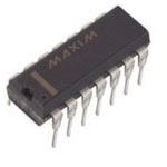
MAX512CPD+
ActiveLOW-COST, TRIPLE, 8-BIT VOLTAGE-OUTPUT DACS WITH SERIAL INTERFACE
MAX512CPD+
ActiveLOW-COST, TRIPLE, 8-BIT VOLTAGE-OUTPUT DACS WITH SERIAL INTERFACE
Description
General part information
MAX512 Series
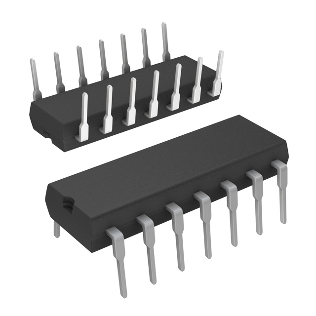
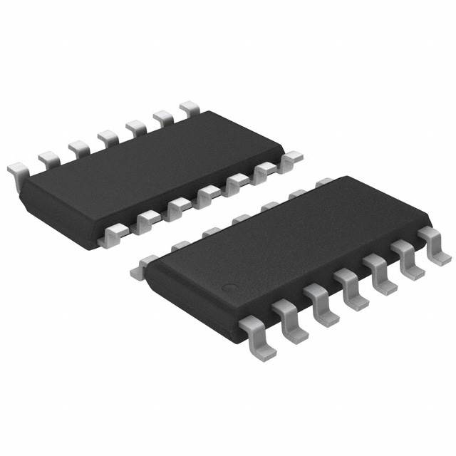
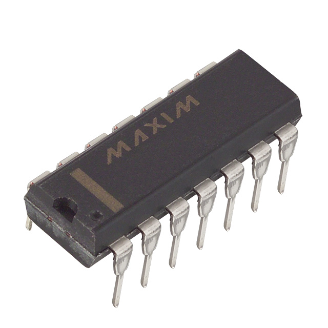
The MAX512/MAX513 contain three 8-bit, voltage-output digital-to-analog converters (DAC A, DAC B, and DAC C). Output buffer amplifiers for DACs A and B provide voltage outputs while reducing external component count. The output buffer for DAC A can source or sink 5mA to within 0.5V of VDDor VSS. The buffer for DAC B can source or sink 0.5mA to within 0.5V of VDDor VSS. DAC C is unbuffered, providing a third voltage output with increased accuracy. The MAX512 operates with a single +5V ±10% supply, and the MAX513 operates with a +2.7V to +3.6V supply. Both devices can also operate with split supplies.The 3-wire serial interface has a maximum operating frequency of 5MHz and is compatible with SPI™, QSPI™, and Microwire™. The serial input shift register is 16 bits long and consists of 8 bits of DAC input data and 8 bits for DAC selection and shutdown. DAC registers can be loaded independently or in parallel at the positive edge of CS. A latched logic output is also available for auxiliary control.Ultra-low power consumption and small packages (14-pin DIP/SO) make the MAX512/MAX513 ideal for portable and battery-powered applications. Supply current is only 1mA, dropping to less than 1µA in shutdown. Any of the three DACs can be independently shut down. In shutdown mode, the DAC's R-2R ladder network is disconnected from the reference input, minimizing system power consumption.ApplicationsDigital Gain and Offset ControlProgrammable AttenuatorsProgrammable Current SourcesProgrammable Voltage SourcesRF Digitally Adjustable Bias CircuitsVCO Tuning
Technical Specifications
Parameters and characteristics for this part
| Specification | MAX512CPD+ |
|---|---|
| Architecture | R-2R |
| Data Interface | SPI |
| Differential Output | No |
| DNL (Max) (LSB) | 1 LSB |
| INL (Max) (LSB) | 1.5 LSB |
| Mounting Type | Through Hole |
| Number of Bits | 8 bits |
| Number of D/A Converters | 3 count |
| Operating Temperature (Max) | 70 °C |
| Operating Temperature (Min) | 0 °C |
| Output Type | Voltage - Buffered |
| Package Length | 0.3 in |
| Package Name | 14-PDIP, 14-DIP |
| Package Width | 7.62 mm |
| Reference Type | External |
| Settling Time (Typical) | 70 µs |
| Voltage - Supply, Analog (Max) | 5 V |
| Voltage - Supply, Analog (Min) | -5 V |
| Voltage - Supply, Digital | 5 V |
Pricing
Prices provided here are for design reference only. For realtime values and availability, please visit the distributors directly
Sign in to see pricing
Create a free account to access distributor pricing data.
CAD
3D models and CAD resources for this part
Documents
Technical documentation and resources