5PB1106PGGI8
ActiveRenesas Electronics Corporation
1.8V TO 3.3V 1:6 LVCMOS HIGH-PERFORMANCE CLOCK BUFFER
5PB1106PGGI8
ActiveRenesas Electronics Corporation
1.8V TO 3.3V 1:6 LVCMOS HIGH-PERFORMANCE CLOCK BUFFER
Description
General part information
5PB1106 Series
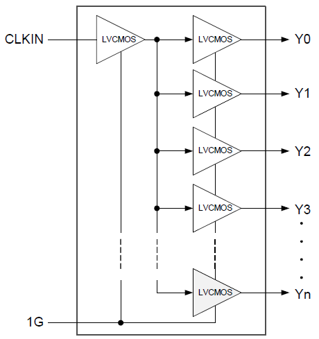
The 5PB1106 is a high-performance 1:6 LVCMOS clock buffer that offers a best-in-class additive phase jitter of 50fs RMS. This clock buffer also supports an Output Enable function. It is available in 16-pin QFN and 14-pin TSSOP packages and can operate from a 1.8V to 3.3V supply.
Technical Specifications
Parameters and characteristics for this part
| Specification | 5PB1106PGGI8 |
|---|---|
| Differential Input | No |
| Differential Output | No |
| Frequency - Max | 200 MHz |
| Input | LVCMOS |
| Input Ratio | 1 |
| Mounting Type | Surface Mount |
| Number of Circuits | 1 |
| Operating Temperature (Max) | 85 °C |
| Operating Temperature (Min) | -40 °C |
| Output | LVCMOS |
| Output Ratio | 6 |
| Package Length | 0.173 in |
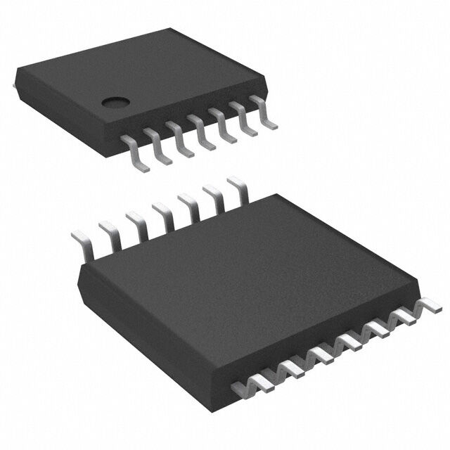
| Package Name | 14-TSSOP |
| Package Width | 4.4 mm |
| Type | Fanout Buffer (Distribution) |
| Voltage - Supply (Range 1 Maximum) | 1.89 V |
| Voltage - Supply (Range 1 Minimum) | 1.71 V |
| Voltage - Supply (Range 2 Maximum) | 2.625 V |
| Voltage - Supply (Range 2 Minimum) | 2.375 V |
| Voltage - Supply (Range 3 Maximum) | 3.465 V |
| Voltage - Supply (Range 3 Minimum) | 3.135 V |
Pricing
Prices provided here are for design reference only. For realtime values and availability, please visit the distributors directly
Sign in to see pricing
Create a free account to access distributor pricing data.
CAD
3D models and CAD resources for this part
Documents
Technical documentation and resources