71V67903S75PFG
Obsolete3.3V 512K X 18 SYNCHRONOUS 3.3V I/O FLOW-THROUGH SRAM
71V67903S75PFG
Obsolete3.3V 512K X 18 SYNCHRONOUS 3.3V I/O FLOW-THROUGH SRAM
Description
General part information
71V67903 Series
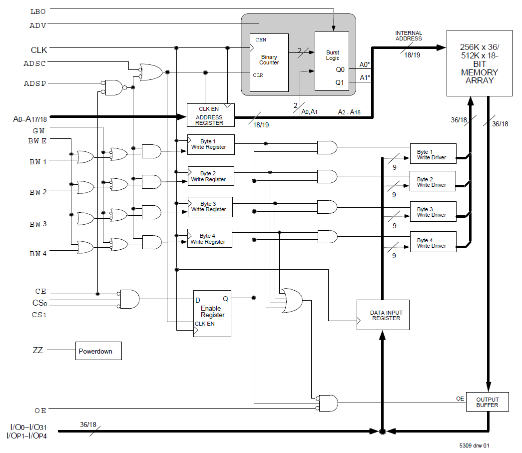
The 71V67903 3.3V CMOS SRAM is organized as 512K x 18. The 71V67903 SRAM contains write, data, address and control registers. There are no registers in the data output path (flow-through architecture). The burst mode feature offers the highest level of performance to the system designer, as it can provide four cycles of data for a single address presented to the SRAM.
Technical Specifications
Parameters and characteristics for this part
| Specification | 71V67903S75PFG |
|---|---|
| Access Time | 7.5 ns |
| Clock Frequency | 117 MHz |
| Memory Depth | 512 K |
| Memory Format | SRAM |
| Memory Interface (Type) | Parallel |
| Memory Size | 9 Mbit |
| Memory Type | Volatile |
| Memory Width | 18 bit |
| Mounting Type | Surface Mount |
| Operating Temperature (Max) | 70 °C |
| Operating Temperature (Min) | 0 °C |
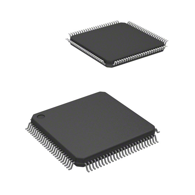
| Package / Case | 100-LQFP |
| Package Length | 14 mm |
| Package Name | 100-TQFP |
| Package Width | 14 mm |
| Technology | SRAM - Synchronous, SDR |
| Voltage - Supply (Maximum) | 3.465 V |
| Voltage - Supply (Minimum) | 3.135 V |
Pricing
Prices provided here are for design reference only. For realtime values and availability, please visit the distributors directly
Sign in to see pricing
Create a free account to access distributor pricing data.
CAD
3D models and CAD resources for this part
Documents
Technical documentation and resources