70V7599S166BF8
Obsolete128K X 36 SYNCHRONOUS BANK-SWITCHABLE DUAL-PORT SRAM
70V7599S166BF8
Obsolete128K X 36 SYNCHRONOUS BANK-SWITCHABLE DUAL-PORT SRAM
Description
General part information
70V7599 Series
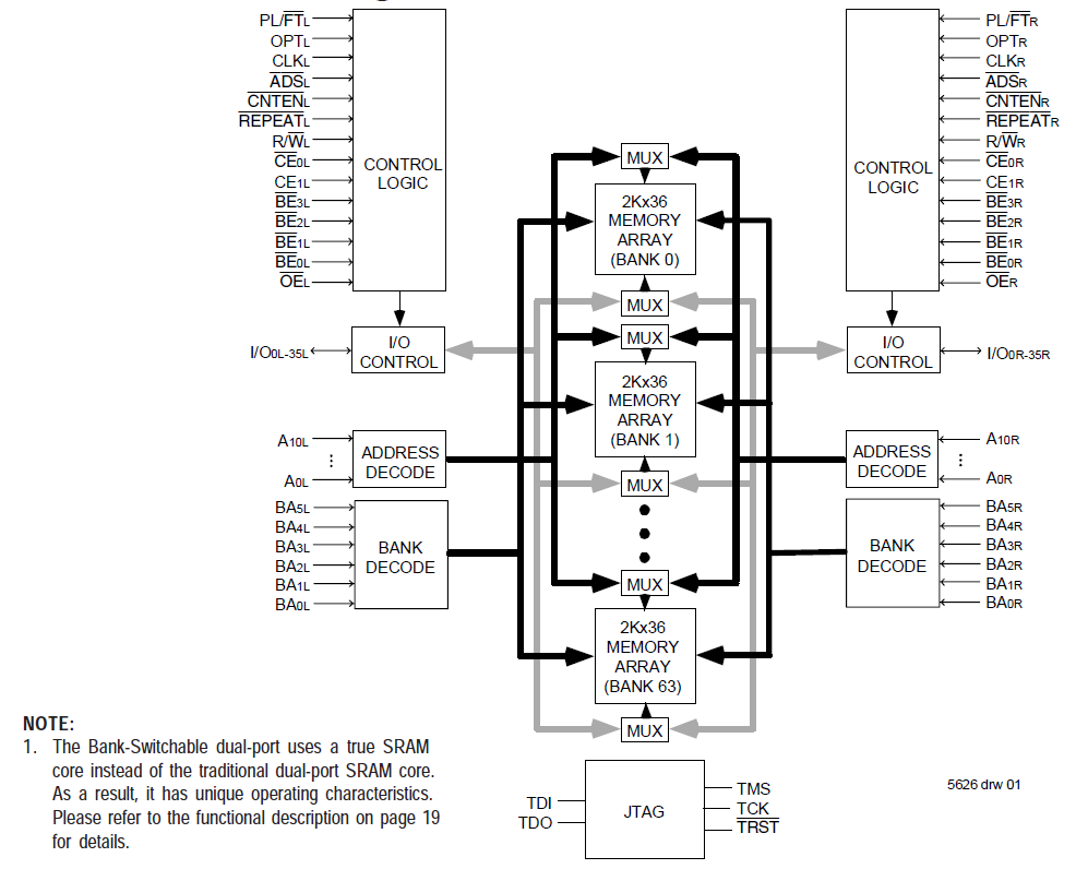
The 70V7599 is a high-speed 128K x 36 (4Mbit) synchronous Bank-Switchable Dual-Ported SRAM is organized into 64 independent 2Kx36 banks and has two independent ports with separate control, address, and I/O pins for each port, allowing each port to access any 2Kx36 memory block not already accessed by the other port. An automatic power down feature, controlled by CE0 and CE1, permits the on-chip circuitry of each port to enter a very low standby power mode.
Technical Specifications
Parameters and characteristics for this part
| Specification | 70V7599S166BF8 |
|---|---|
| Access Time | 3.6 ns |
| Clock Frequency | 166 MHz |
| Memory Depth | 128 K |
| Memory Format | SRAM |
| Memory Interface (Type) | Parallel |
| Memory Size | 4.5 Mbit |
| Memory Type | Volatile |
| Memory Width | 36 bit |
| Mounting Type | Surface Mount |
| Operating Temperature (Max) | 70 °C |
| Operating Temperature (Min) | 0 °C |
| Package / Case | 208-LFBGA |
| Package Length | 15 mm |
| Package Name | 208-CABGA |
| Package Width | 15 mm |
| Technology | Synchronous, SRAM - Dual Port |
| Voltage - Supply (Maximum) | 3.45 V |
| Voltage - Supply (Minimum) | 3.15 V |
Pricing
Prices provided here are for design reference only. For realtime values and availability, please visit the distributors directly
Sign in to see pricing
Create a free account to access distributor pricing data.
CAD
3D models and CAD resources for this part
Documents
Technical documentation and resources