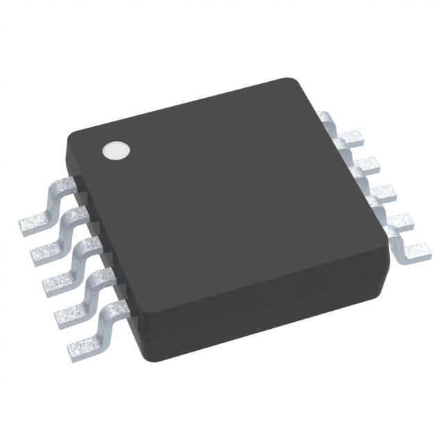
ADC122S625CIMM/NOPB
ActiveDUAL 12-BIT, 50 KSPS TO 200 KSPS, SIMULTANEOUS SAMPLING A/D CONVERTER
Deep-Dive with AI
Search across all available documentation for this part.

ADC122S625CIMM/NOPB
ActiveDUAL 12-BIT, 50 KSPS TO 200 KSPS, SIMULTANEOUS SAMPLING A/D CONVERTER
Technical Specifications
Parameters and characteristics commom to parts in this series
| Specification | ADC122S625CIMM/NOPB | ADC122S625 Series |
|---|---|---|
| Architecture | SAR | SAR |
| Configuration | S/H-ADC | S/H-ADC |
| Data Interface | SPI, DSP | SPI, DSP |
| Features | Simultaneous Sampling | Simultaneous Sampling |
| Input Type | Differential, Single Ended | Differential, Single Ended |
| Mounting Type | Surface Mount | Surface Mount |
| Number of A/D Converters | 2 | 2 |
| Number of Bits | 12 | 12 |
| Number of Inputs | 2 | 2 |
| Operating Temperature [Max] | 105 ░C | 105 ░C |
| Operating Temperature [Min] | -40 °C | -40 °C |
| Package / Case | 10-TFSOP, 10-MSOP | 10-TFSOP, 10-MSOP |
| Ratio - S/H:ADC | 1:1 | 1:1 |
| Reference Type | External | External |
| Sampling Rate (Per Second) | 200k | 200k |
| Supplier Device Package | 10-VSSOP | 10-VSSOP |
| Voltage - Supply, Analog | 5 V | 5 V |
| Voltage - Supply, Digital | 5 V | 5 V |
Pricing
Prices provided here are for design reference only. For realtime values and availability, please visit the distributors directly
ADC122S625 Series
Dual 12-Bit, 50 kSPS to 200 kSPS, Simultaneous Sampling A/D Converter
| Part | Voltage - Supply, Digital | Mounting Type | Number of Bits | Number of Inputs | Voltage - Supply, Analog | Sampling Rate (Per Second) | Input Type | Architecture | Reference Type | Number of A/D Converters | Operating Temperature [Min] | Operating Temperature [Max] | Supplier Device Package | Features | Ratio - S/H:ADC | Package / Case | Data Interface | Configuration |
|---|---|---|---|---|---|---|---|---|---|---|---|---|---|---|---|---|---|---|
Texas Instruments ADC122S625CIMM/NOPBThe ADC122S625 is a dual 12-bit, 50 kSPS to 200 kSPS simultaneous sampling Analog-to-Digital (A/D) converter. The analog inputs on both channels are sampled simultaneously to preserve their relative phase information to each other. The converter is based on a successive-approximation register architecture where the differential nature of the analog inputs is maintained from the internal track-and-hold circuits throughout the A/D converter to provide excellent common-mode signal rejection. The ADC122S625 features an external reference that can be varied from 1.0V to VA.
The ADC122S625's serial data output is binary 2's complement and is compatible with several standards, such as SPI™, QSPI™, MICROWIRE™, and many common DSP serial interfaces. The serial clock (SCLK) and chip select bar (CS) are shared by both channels.
Operating from a single 5V analog supply and a reference voltage of 2.5V, the total power consumption while operating at 200 kSPS is typically 8.6 mW. With the ADC122S625 operating in power-down mode, the power consumption reduces to 2.6 µW. The differential input, low power consumption, and small size make the ADC122S625 ideal for direct connection to sensors in motor control applications.
Operation is specified over the industrial temperature range of −40°C to +105°C and clock rates of 1.6 MHz to 6.4 MHz. The ADC122S625 is available in a 10-lead VSSOP package.
The ADC122S625 is a dual 12-bit, 50 kSPS to 200 kSPS simultaneous sampling Analog-to-Digital (A/D) converter. The analog inputs on both channels are sampled simultaneously to preserve their relative phase information to each other. The converter is based on a successive-approximation register architecture where the differential nature of the analog inputs is maintained from the internal track-and-hold circuits throughout the A/D converter to provide excellent common-mode signal rejection. The ADC122S625 features an external reference that can be varied from 1.0V to VA.
The ADC122S625's serial data output is binary 2's complement and is compatible with several standards, such as SPI™, QSPI™, MICROWIRE™, and many common DSP serial interfaces. The serial clock (SCLK) and chip select bar (CS) are shared by both channels.
Operating from a single 5V analog supply and a reference voltage of 2.5V, the total power consumption while operating at 200 kSPS is typically 8.6 mW. With the ADC122S625 operating in power-down mode, the power consumption reduces to 2.6 µW. The differential input, low power consumption, and small size make the ADC122S625 ideal for direct connection to sensors in motor control applications.
Operation is specified over the industrial temperature range of −40°C to +105°C and clock rates of 1.6 MHz to 6.4 MHz. The ADC122S625 is available in a 10-lead VSSOP package. | 5 V | Surface Mount | 12 | 2 | 5 V | 200k | Differential, Single Ended | SAR | External | 2 | -40 °C | 105 ░C | 10-VSSOP | Simultaneous Sampling | 1:1 | 10-MSOP, 10-TFSOP | DSP, SPI | S/H-ADC |
Texas Instruments ADC122S625CIMMX/NOPBThe ADC122S625 is a dual 12-bit, 50 kSPS to 200 kSPS simultaneous sampling Analog-to-Digital (A/D) converter. The analog inputs on both channels are sampled simultaneously to preserve their relative phase information to each other. The converter is based on a successive-approximation register architecture where the differential nature of the analog inputs is maintained from the internal track-and-hold circuits throughout the A/D converter to provide excellent common-mode signal rejection. The ADC122S625 features an external reference that can be varied from 1.0V to VA.
The ADC122S625's serial data output is binary 2's complement and is compatible with several standards, such as SPI™, QSPI™, MICROWIRE™, and many common DSP serial interfaces. The serial clock (SCLK) and chip select bar (CS) are shared by both channels.
Operating from a single 5V analog supply and a reference voltage of 2.5V, the total power consumption while operating at 200 kSPS is typically 8.6 mW. With the ADC122S625 operating in power-down mode, the power consumption reduces to 2.6 µW. The differential input, low power consumption, and small size make the ADC122S625 ideal for direct connection to sensors in motor control applications.
Operation is specified over the industrial temperature range of −40°C to +105°C and clock rates of 1.6 MHz to 6.4 MHz. The ADC122S625 is available in a 10-lead VSSOP package.
The ADC122S625 is a dual 12-bit, 50 kSPS to 200 kSPS simultaneous sampling Analog-to-Digital (A/D) converter. The analog inputs on both channels are sampled simultaneously to preserve their relative phase information to each other. The converter is based on a successive-approximation register architecture where the differential nature of the analog inputs is maintained from the internal track-and-hold circuits throughout the A/D converter to provide excellent common-mode signal rejection. The ADC122S625 features an external reference that can be varied from 1.0V to VA.
The ADC122S625's serial data output is binary 2's complement and is compatible with several standards, such as SPI™, QSPI™, MICROWIRE™, and many common DSP serial interfaces. The serial clock (SCLK) and chip select bar (CS) are shared by both channels.
Operating from a single 5V analog supply and a reference voltage of 2.5V, the total power consumption while operating at 200 kSPS is typically 8.6 mW. With the ADC122S625 operating in power-down mode, the power consumption reduces to 2.6 µW. The differential input, low power consumption, and small size make the ADC122S625 ideal for direct connection to sensors in motor control applications.
Operation is specified over the industrial temperature range of −40°C to +105°C and clock rates of 1.6 MHz to 6.4 MHz. The ADC122S625 is available in a 10-lead VSSOP package. | 5 V | Surface Mount | 12 | 2 | 5 V | 200k | Differential, Single Ended | SAR | External | 2 | -40 °C | 105 ░C | 10-VSSOP | Simultaneous Sampling | 1:1 | 10-MSOP, 10-TFSOP | DSP, SPI | S/H-ADC |
Description
General part information
ADC122S625 Series
The ADC122S625 is a dual 12-bit, 50 kSPS to 200 kSPS simultaneous sampling Analog-to-Digital (A/D) converter. The analog inputs on both channels are sampled simultaneously to preserve their relative phase information to each other. The converter is based on a successive-approximation register architecture where the differential nature of the analog inputs is maintained from the internal track-and-hold circuits throughout the A/D converter to provide excellent common-mode signal rejection. The ADC122S625 features an external reference that can be varied from 1.0V to VA.
The ADC122S625's serial data output is binary 2's complement and is compatible with several standards, such as SPI™, QSPI™, MICROWIRE™, and many common DSP serial interfaces. The serial clock (SCLK) and chip select bar (CS) are shared by both channels.
Operating from a single 5V analog supply and a reference voltage of 2.5V, the total power consumption while operating at 200 kSPS is typically 8.6 mW. With the ADC122S625 operating in power-down mode, the power consumption reduces to 2.6 µW. The differential input, low power consumption, and small size make the ADC122S625 ideal for direct connection to sensors in motor control applications.


