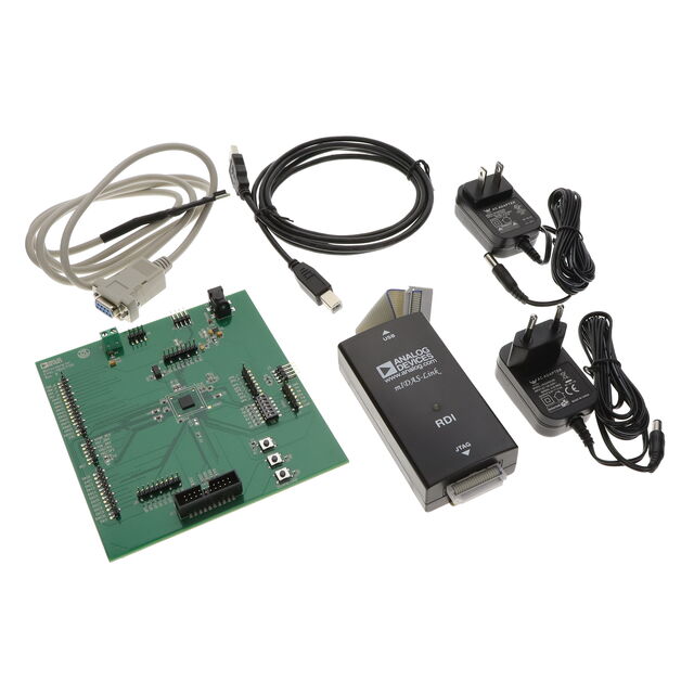
ADUC7120BBCZ-RL
ActivePRECISION ANALOG MICROCONTROLLER, 12-BIT ANALOG INPUT/OUTPUT, ARM7TDMI MCU
ADUC7120BBCZ-RL
ActivePRECISION ANALOG MICROCONTROLLER, 12-BIT ANALOG INPUT/OUTPUT, ARM7TDMI MCU
Description
General part information
ADUC7120 Series
The ADuC7120/ADuC7121are fully integrated, 12-bit, 1 MSPS, data acquisition systems incorporating a high performance multichannel ADC, 16-bit/32-bit microcontroller unit (MCU), and Flash®/EE memory on a single chip.The analog-to-digital converter (ADC) consists of eleven single-ended inputs for the ADuC7120 (seven single-ended inputs for the ADuC7121) and two extra differential input pairs. The two differential input pairs can be routed through a programmable gain amplifier (PGA). The ADC can operate in single-ended or differential input mode. The ADC input voltage is 0 V to VREF. A low drift band gap reference, temperature sensor, and voltage comparator complete the ADC peripheral set.The ADuC7120/ADuC7121 provide five current output digital-to-analog converters (DACs). The current sources (five current DACs) feature low noise and low drift, high-side current output at an 11-bit resolution. The five current digital-to-analog converters (IDACs) are as follows: IDAC0 with 250 mA full-scale (FS) output, IDAC1 with 200 mA FS output, IDAC2 with 45 mA FS output, IDAC3 with 80 mA FS output, and IDAC4 with 20 mA FS output.The ADuC7120/ADuC7121 also contain up to 12 voltage output DACs. The DAC output range is programmable to one of three voltage ranges.The devices operate from an on-chip oscillator and a phase-locked loop (PLL) generating an internal high frequency clock of 41.78 MHz (UCLK). This clock is routed through a programmable clock divider from which the MCU core clock operating frequency is generated. The microcontroller core is an ARM7TDMI®, 16-bit/32-bit reduced instruction set computer (RISC) machine, which offers up to 41 MIPS peak performance. 8 kB of SRAM and 126 kB of nonvolatile Flash/EE memory are provided on chip. The ARM7TDMI core views all memory and registers as a single linear array.On-chip factory firmware supports in circuit serial download via the I2C serial interface port; nonintrusive emulation is also supported via the JTAG interface. These features are incorporated into a low costQuickStartdevelopment system supporting this MicroConverter®family.The devices operate from 3.0 V to 3.6 V, and they are specified over the −40°C to +105°C industrial temperature range. The IDACs are powered from a separate input power supply, PVDD. When operating at 41.78 MHz, the power dissipation is typically 120 mW. The ADuC7120/ADuC7121 are available in a 108-ball chip-scale package ball grid array [CSP_BGA].ApplicationsOptical modules—tunable laser
Technical Specifications
Parameters and characteristics for this part
| Specification | ADUC7120BBCZ-RL |
|---|---|
| A/D Channels | 11 count |
| A/D Resolution (bits) | 12 bit |
| Connectivity | USART, UART, SPI, I2C |
| Core Processor | ARM7® |
| Core Size (Bit Width Options) | 16-Bit, 32-Bit |
| D/A Channels | 12 count |
| D/A Resolution (bits) | 12 bit |
| Mounting Type | Surface Mount |
| Number of I/O | 32 |
| Operating Temperature (Max) | 105 °C |
| Operating Temperature (Min) | -40 °C |
| Oscillator Type | Internal |
| Package / Case | CSPBGA, 108-LFBGA |
| Package Length | 7 mm |
| Package Name | 108-CSPBGA |
| Package Width | 7 mm |
| Peripherals | WDT, POR, PWM |
| Program Memory Depth | 63 K |
| Program Memory Size | 126 KB |
| Program Memory Type | FLASH |
| Program Memory Width | 16 |
| RAM Size Depth | 2 K |
| RAM Size Width | 32 bit |
| Speed | 41.78 MHz |
| Voltage - Supply (Vcc/Vdd) Maximum | 3.6 V |
| Voltage - Supply (Vcc/Vdd) Minimum | 3 V |
Pricing
Prices provided here are for design reference only. For realtime values and availability, please visit the distributors directly
Sign in to see pricing
Create a free account to access distributor pricing data.
CAD
3D models and CAD resources for this part
Documents
Technical documentation and resources