49FCT805APYG8
ObsoleteFAST CMOS BUFFER/CLOCK DRIVER
49FCT805APYG8
ObsoleteFAST CMOS BUFFER/CLOCK DRIVER
Description
General part information
49FCT805 Series
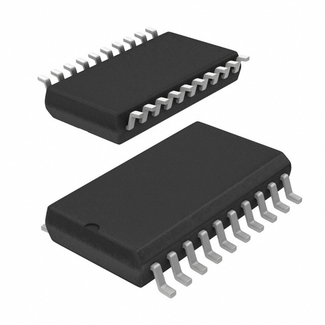
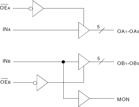
The 49FCT805 is a non-inverting buffer/clock driver built using advanced dual metal CMOS technology. Each bank consists of two banks of drivers. Each bank drives five output buffers from a standard TTL compatible input. These devices feature a "heart-beat" monitor for diagnostics and PLL driving. The MON output is identical to all other outputs and complies with the output specifications in this document. The 49FCT805 offers low capacitance inputs and hysteresis. Rail-to-rail output swing improves noise margin and allows easy interface with CMOS inputs.
Technical Specifications
Parameters and characteristics for this part
| Specification | 49FCT805APYG8 |
|---|---|
| Differential Input | No |
| Differential Output | No |
| Input | CMOS, LVTTL |
| Input Ratio | 1 |
| Mounting Type | Surface Mount |
| Number of Circuits | 2 |
| Operating Temperature (Max) | 70 °C |
| Operating Temperature (Min) | 0 °C |
| Output | CMOS, LVTTL |
| Output Ratio | 5 |
| Package Length | 0.209 in |
| Package Name | 20-SSOP |
| Package Width | 5.3 mm |
| Type | Fanout Buffer (Distribution) |
| Voltage - Supply (Maximum) | 5.25 V |
| Voltage - Supply (Minimum) | 4.75 V |
Pricing
Prices provided here are for design reference only. For realtime values and availability, please visit the distributors directly
Sign in to see pricing
Create a free account to access distributor pricing data.
CAD
3D models and CAD resources for this part
Documents
Technical documentation and resources