ADC10D1500CIUT/NOPB
Active10-BIT, DUAL 1.5-GSPS OR SINGLE 3.0-GSPS ANALOG-TO-DIGITAL CONVERTER (ADC)
Deep-Dive with AI
Search across all available documentation for this part.
ADC10D1500CIUT/NOPB
Active10-BIT, DUAL 1.5-GSPS OR SINGLE 3.0-GSPS ANALOG-TO-DIGITAL CONVERTER (ADC)
Technical Specifications
Parameters and characteristics commom to parts in this series
| Specification | ADC10D1500CIUT/NOPB | ADC10D1500 Series |
|---|---|---|
| Architecture | Folding Interpolating | Folding Interpolating |
| Configuration | MUX-S/H-ADC | MUX-S/H-ADC |
| Data Interface | LVDS - Parallel | LVDS - Parallel |
| Features | Simultaneous Sampling | Simultaneous Sampling |
| Input Type | Differential | Differential |
| Mounting Type | Surface Mount | Surface Mount |
| Number of A/D Converters | 2 | 2 |
| Number of Bits | 10 | 10 |
| Number of Inputs | 2 | 2 |
| Operating Temperature [Max] | 70 ░C | 70 ░C |
| Operating Temperature [Min] | -40 °C | -40 °C |
| Package / Case | 292-BBGA | 292-BBGA |
| Ratio - S/H:ADC | 1:1 | 1:1 |
| Reference Type | Internal | Internal |
| Sampling Rate (Per Second) | 1.5 G | 1.5 G |
| Supplier Device Package | 292-BGA | 292-BGA |
| Voltage - Supply, Analog [Max] | 2 V | 2 V |
| Voltage - Supply, Analog [Min] | 1.8 V | 1.8 V |
| Voltage - Supply, Digital [Max] | 2 V | 2 V |
| Voltage - Supply, Digital [Min] | 1.8 V | 1.8 V |
Pricing
Prices provided here are for design reference only. For realtime values and availability, please visit the distributors directly
ADC10D1500 Series
10-Bit, Dual 1.5-GSPS or Single 3.0-GSPS Analog-to-Digital Converter (ADC)
| Part | Supplier Device Package | Number of Bits | Data Interface | Number of Inputs | Voltage - Supply, Analog [Min] | Voltage - Supply, Analog [Max] | Operating Temperature [Max] | Operating Temperature [Min] | Ratio - S/H:ADC | Sampling Rate (Per Second) | Features | Reference Type | Voltage - Supply, Digital [Min] | Voltage - Supply, Digital [Max] | Mounting Type | Configuration | Package / Case | Architecture | Number of A/D Converters | Input Type |
|---|---|---|---|---|---|---|---|---|---|---|---|---|---|---|---|---|---|---|---|---|
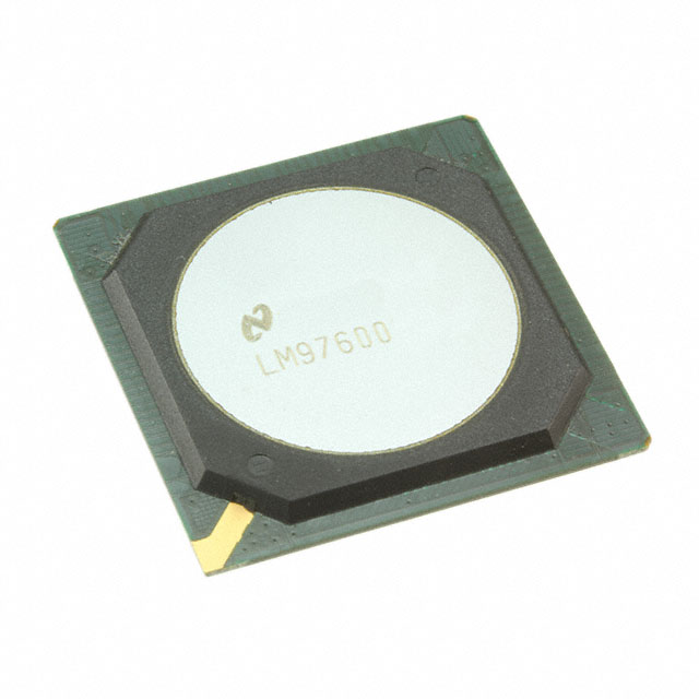
Texas Instruments ADC10D1500CIUTThe ADC10D1000/1500 is the latest advance in TI's Ultra-High-Speed ADC family. This low-power, high-performance CMOS analog-to-digital converter digitizes signals at 10-bit resolution for dual channels at sampling rates of up to 1.0/1.5 GSPS (Non-DES Mode) or for a single channel up to 2.0/3.0 GSPS (DES Mode). The ADC10D1000/1500 achieves excellent accuracy and dynamic performance while dissipating less than 2.8/3.6 Watts. The product is packaged in a leaded or lead-free 292-ball thermally enhanced BGA package over the rated industrial temperature range of -40°C to +85°C.
The ADC10D1000/1500 builds upon the features, architecture and functionality of the 8-bit GHz family of ADCs. An expanded feature set includes AutoSync for multi-chip synchronization, 15-bit programmable gain and 12-bit plus sign programmable offset adjustment for each channel. The improved internal track-and-hold amplifier and the extended self-calibration scheme enable a very flat response of all dynamic parameters beyond Nyquist, producing 9.1/9.0 Effective Number of Bits (ENOB) with a 100 MHz input signal and a 1.0/1.5 GHz sample rate while providing a 10-18Code Error Rate (CER) Dissipating a typical 2.77/3.59 Watts in Non-Demultiplex Mode at 1.0/1.5 GSPS from a single 1.9V supply, this device is specified to have no missing codes over the full operating temperature range.
Each channel has its own independent DDR Data Clock, DCLKI and DCLKQ, which are in phase when both channels are powered up, so that only one Data Clock could be used to capture all data, which is sent out at the same rate as the input sample clock. If the 1:2 Demux Mode is selected, a second 10-bit LVDS bus becomes active for each channel, such that the output data rate is sent out two times slower to relax data-capture timing requirements. The part can also be used as a single 2.0/3.0 GSPS ADC to sample one of the I or Q inputs. The output formatting can be programmed to be offset binary or two's complement and the Low Voltage Differential Signaling (LVDS) digital outputs are compatible with IEEE 1596.3-1996, with the exception of an adjustable common mode voltage between 0.8V and 1.2V to allow for power reduction for well-controlled back planes.
The ADC10D1000/1500 is the latest advance in TI's Ultra-High-Speed ADC family. This low-power, high-performance CMOS analog-to-digital converter digitizes signals at 10-bit resolution for dual channels at sampling rates of up to 1.0/1.5 GSPS (Non-DES Mode) or for a single channel up to 2.0/3.0 GSPS (DES Mode). The ADC10D1000/1500 achieves excellent accuracy and dynamic performance while dissipating less than 2.8/3.6 Watts. The product is packaged in a leaded or lead-free 292-ball thermally enhanced BGA package over the rated industrial temperature range of -40°C to +85°C.
The ADC10D1000/1500 builds upon the features, architecture and functionality of the 8-bit GHz family of ADCs. An expanded feature set includes AutoSync for multi-chip synchronization, 15-bit programmable gain and 12-bit plus sign programmable offset adjustment for each channel. The improved internal track-and-hold amplifier and the extended self-calibration scheme enable a very flat response of all dynamic parameters beyond Nyquist, producing 9.1/9.0 Effective Number of Bits (ENOB) with a 100 MHz input signal and a 1.0/1.5 GHz sample rate while providing a 10-18Code Error Rate (CER) Dissipating a typical 2.77/3.59 Watts in Non-Demultiplex Mode at 1.0/1.5 GSPS from a single 1.9V supply, this device is specified to have no missing codes over the full operating temperature range.
Each channel has its own independent DDR Data Clock, DCLKI and DCLKQ, which are in phase when both channels are powered up, so that only one Data Clock could be used to capture all data, which is sent out at the same rate as the input sample clock. If the 1:2 Demux Mode is selected, a second 10-bit LVDS bus becomes active for each channel, such that the output data rate is sent out two times slower to relax data-capture timing requirements. The part can also be used as a single 2.0/3.0 GSPS ADC to sample one of the I or Q inputs. The output formatting can be programmed to be offset binary or two's complement and the Low Voltage Differential Signaling (LVDS) digital outputs are compatible with IEEE 1596.3-1996, with the exception of an adjustable common mode voltage between 0.8V and 1.2V to allow for power reduction for well-controlled back planes. | 292-BGA | 10 | LVDS - Parallel | 2 | 1.8 V | 2 V | 70 ░C | -40 °C | 1:1 | 1.5 G | Simultaneous Sampling | Internal | 1.8 V | 2 V | Surface Mount | MUX-S/H-ADC | 292-BBGA | Folding Interpolating | 2 | Differential |
Texas Instruments ADC10D1500CIUT/NOPBThe ADC10D1000/1500 is the latest advance in TI's Ultra-High-Speed ADC family. This low-power, high-performance CMOS analog-to-digital converter digitizes signals at 10-bit resolution for dual channels at sampling rates of up to 1.0/1.5 GSPS (Non-DES Mode) or for a single channel up to 2.0/3.0 GSPS (DES Mode). The ADC10D1000/1500 achieves excellent accuracy and dynamic performance while dissipating less than 2.8/3.6 Watts. The product is packaged in a leaded or lead-free 292-ball thermally enhanced BGA package over the rated industrial temperature range of -40°C to +85°C.
The ADC10D1000/1500 builds upon the features, architecture and functionality of the 8-bit GHz family of ADCs. An expanded feature set includes AutoSync for multi-chip synchronization, 15-bit programmable gain and 12-bit plus sign programmable offset adjustment for each channel. The improved internal track-and-hold amplifier and the extended self-calibration scheme enable a very flat response of all dynamic parameters beyond Nyquist, producing 9.1/9.0 Effective Number of Bits (ENOB) with a 100 MHz input signal and a 1.0/1.5 GHz sample rate while providing a 10-18Code Error Rate (CER) Dissipating a typical 2.77/3.59 Watts in Non-Demultiplex Mode at 1.0/1.5 GSPS from a single 1.9V supply, this device is specified to have no missing codes over the full operating temperature range.
Each channel has its own independent DDR Data Clock, DCLKI and DCLKQ, which are in phase when both channels are powered up, so that only one Data Clock could be used to capture all data, which is sent out at the same rate as the input sample clock. If the 1:2 Demux Mode is selected, a second 10-bit LVDS bus becomes active for each channel, such that the output data rate is sent out two times slower to relax data-capture timing requirements. The part can also be used as a single 2.0/3.0 GSPS ADC to sample one of the I or Q inputs. The output formatting can be programmed to be offset binary or two's complement and the Low Voltage Differential Signaling (LVDS) digital outputs are compatible with IEEE 1596.3-1996, with the exception of an adjustable common mode voltage between 0.8V and 1.2V to allow for power reduction for well-controlled back planes.
The ADC10D1000/1500 is the latest advance in TI's Ultra-High-Speed ADC family. This low-power, high-performance CMOS analog-to-digital converter digitizes signals at 10-bit resolution for dual channels at sampling rates of up to 1.0/1.5 GSPS (Non-DES Mode) or for a single channel up to 2.0/3.0 GSPS (DES Mode). The ADC10D1000/1500 achieves excellent accuracy and dynamic performance while dissipating less than 2.8/3.6 Watts. The product is packaged in a leaded or lead-free 292-ball thermally enhanced BGA package over the rated industrial temperature range of -40°C to +85°C.
The ADC10D1000/1500 builds upon the features, architecture and functionality of the 8-bit GHz family of ADCs. An expanded feature set includes AutoSync for multi-chip synchronization, 15-bit programmable gain and 12-bit plus sign programmable offset adjustment for each channel. The improved internal track-and-hold amplifier and the extended self-calibration scheme enable a very flat response of all dynamic parameters beyond Nyquist, producing 9.1/9.0 Effective Number of Bits (ENOB) with a 100 MHz input signal and a 1.0/1.5 GHz sample rate while providing a 10-18Code Error Rate (CER) Dissipating a typical 2.77/3.59 Watts in Non-Demultiplex Mode at 1.0/1.5 GSPS from a single 1.9V supply, this device is specified to have no missing codes over the full operating temperature range.
Each channel has its own independent DDR Data Clock, DCLKI and DCLKQ, which are in phase when both channels are powered up, so that only one Data Clock could be used to capture all data, which is sent out at the same rate as the input sample clock. If the 1:2 Demux Mode is selected, a second 10-bit LVDS bus becomes active for each channel, such that the output data rate is sent out two times slower to relax data-capture timing requirements. The part can also be used as a single 2.0/3.0 GSPS ADC to sample one of the I or Q inputs. The output formatting can be programmed to be offset binary or two's complement and the Low Voltage Differential Signaling (LVDS) digital outputs are compatible with IEEE 1596.3-1996, with the exception of an adjustable common mode voltage between 0.8V and 1.2V to allow for power reduction for well-controlled back planes. | 292-BGA | 10 | LVDS - Parallel | 2 | 1.8 V | 2 V | 70 ░C | -40 °C | 1:1 | 1.5 G | Simultaneous Sampling | Internal | 1.8 V | 2 V | Surface Mount | MUX-S/H-ADC | 292-BBGA | Folding Interpolating | 2 | Differential |
Description
General part information
ADC10D1500 Series
The ADC10D1000/1500 is the latest advance in TI's Ultra-High-Speed ADC family. This low-power, high-performance CMOS analog-to-digital converter digitizes signals at 10-bit resolution for dual channels at sampling rates of up to 1.0/1.5 GSPS (Non-DES Mode) or for a single channel up to 2.0/3.0 GSPS (DES Mode). The ADC10D1000/1500 achieves excellent accuracy and dynamic performance while dissipating less than 2.8/3.6 Watts. The product is packaged in a leaded or lead-free 292-ball thermally enhanced BGA package over the rated industrial temperature range of -40°C to +85°C.
The ADC10D1000/1500 builds upon the features, architecture and functionality of the 8-bit GHz family of ADCs. An expanded feature set includes AutoSync for multi-chip synchronization, 15-bit programmable gain and 12-bit plus sign programmable offset adjustment for each channel. The improved internal track-and-hold amplifier and the extended self-calibration scheme enable a very flat response of all dynamic parameters beyond Nyquist, producing 9.1/9.0 Effective Number of Bits (ENOB) with a 100 MHz input signal and a 1.0/1.5 GHz sample rate while providing a 10-18Code Error Rate (CER) Dissipating a typical 2.77/3.59 Watts in Non-Demultiplex Mode at 1.0/1.5 GSPS from a single 1.9V supply, this device is specified to have no missing codes over the full operating temperature range.
Each channel has its own independent DDR Data Clock, DCLKI and DCLKQ, which are in phase when both channels are powered up, so that only one Data Clock could be used to capture all data, which is sent out at the same rate as the input sample clock. If the 1:2 Demux Mode is selected, a second 10-bit LVDS bus becomes active for each channel, such that the output data rate is sent out two times slower to relax data-capture timing requirements. The part can also be used as a single 2.0/3.0 GSPS ADC to sample one of the I or Q inputs. The output formatting can be programmed to be offset binary or two's complement and the Low Voltage Differential Signaling (LVDS) digital outputs are compatible with IEEE 1596.3-1996, with the exception of an adjustable common mode voltage between 0.8V and 1.2V to allow for power reduction for well-controlled back planes.
Documents
Technical documentation and resources