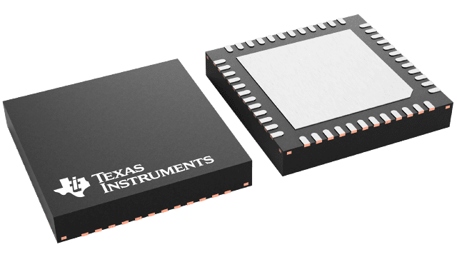
CDCDB800RSLT
Active8-OUTPUT CLOCK BUFFER FOR PCIE® GEN 1 TO GEN 6
Deep-Dive with AI
Search across all available documentation for this part.

CDCDB800RSLT
Active8-OUTPUT CLOCK BUFFER FOR PCIE® GEN 1 TO GEN 6
Technical Specifications
Parameters and characteristics commom to parts in this series
| Specification | CDCDB800RSLT | CDCDB800 Series |
|---|---|---|
| Differential - Input:Output [custom] | True | True |
| Differential - Input:Output [custom] | True | True |
| Frequency - Max [Max] | 250 MHz | 250 MHz |
| Input | HCSL | HCSL |
| Mounting Type | Surface Mount | Surface Mount |
| Number of Circuits | 1 | 1 |
| Operating Temperature [Max] | 105 °C | 105 °C |
| Operating Temperature [Min] | -40 °C | -40 °C |
| Output | Clock, HCSL | Clock, HCSL |
| Package / Case | 48-VFQFN Exposed Pad | 48-VFQFN Exposed Pad |
| Ratio - Input:Output [custom] | 1 | 1 |
| Ratio - Input:Output [custom] | 8 | 8 |
| Supplier Device Package | 48-VQFN (6x6) | 48-VQFN (6x6) |
| Type | Clock Buffer | Clock Buffer |
| Voltage - Supply [Max] | 3.6 V | 3.6 V |
| Voltage - Supply [Min] | 3 V | 3 V |
Pricing
Prices provided here are for design reference only. For realtime values and availability, please visit the distributors directly
| Distributor | Package | Quantity | $ | |
|---|---|---|---|---|
| Digikey | Tape & Reel (TR) | 250 | $ 4.13 | |
| 500 | $ 3.70 | |||
| 1250 | $ 3.12 | |||
| 2500 | $ 2.97 | |||
| Texas Instruments | SMALL T&R | 1 | $ 4.46 | |
| 100 | $ 3.91 | |||
| 250 | $ 2.74 | |||
| 1000 | $ 2.21 | |||
CDCDB800 Series
8-output clock buffer for PCIe® Gen 1 to Gen 6
| Part | Package / Case | Ratio - Input:Output [custom] | Ratio - Input:Output [custom] | Voltage - Supply [Max] | Voltage - Supply [Min] | Input | Supplier Device Package | Output | Mounting Type | Type | Differential - Input:Output [custom] | Differential - Input:Output [custom] | Operating Temperature [Max] | Operating Temperature [Min] | Number of Circuits | Frequency - Max [Max] |
|---|---|---|---|---|---|---|---|---|---|---|---|---|---|---|---|---|
Texas Instruments CDCDB800RSLT | 48-VFQFN Exposed Pad | 1 | 8 | 3.6 V | 3 V | HCSL | 48-VQFN (6x6) | Clock, HCSL | Surface Mount | Clock Buffer | 105 °C | -40 °C | 1 | 250 MHz | ||
Texas Instruments CDCDB800RSLR | 48-VFQFN Exposed Pad | 1 | 8 | 3.6 V | 3 V | HCSL | 48-VQFN (6x6) | Clock, HCSL | Surface Mount | Clock Buffer | 105 °C | -40 °C | 1 | 250 MHz |
Description
General part information
CDCDB800 Series
The CDCDB800 is a 8-output LP-HCSL, DB800ZL-compliant, clock buffer capable of distributing the reference clock for PCIe Gen 1-6, QuickPath Interconnect (QPI), UPI, SAS, and SATA interfaces. The SMBus interface and eight output enable pins allow the configuration and control of all eight outputs individually. The CDCDB800 is a DB800ZL derivative buffer and meets or exceeds the system parameters in the DB800ZL specification. It also meets or exceeds the parameters in the DB2000Q specification. The CDCDB800 is packaged in a 6-mm × 6-mm, 48-pin VQFN package.
The CDCDB800 is a 8-output LP-HCSL, DB800ZL-compliant, clock buffer capable of distributing the reference clock for PCIe Gen 1-6, QuickPath Interconnect (QPI), UPI, SAS, and SATA interfaces. The SMBus interface and eight output enable pins allow the configuration and control of all eight outputs individually. The CDCDB800 is a DB800ZL derivative buffer and meets or exceeds the system parameters in the DB800ZL specification. It also meets or exceeds the parameters in the DB2000Q specification. The CDCDB800 is packaged in a 6-mm × 6-mm, 48-pin VQFN package.


