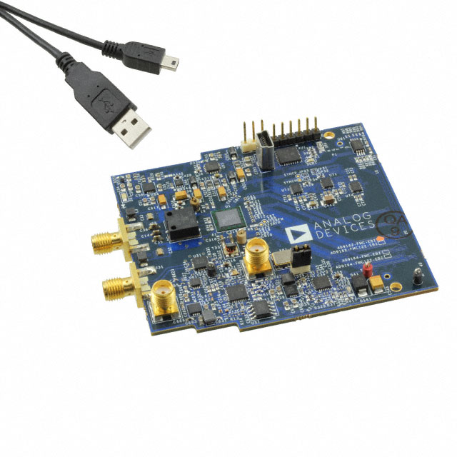
AD9162BBCA
UnknownDIGITAL TO ANALOG CONVERTERS - DAC GENERAL PURPOSE 5 GHZ RFDAC
AD9162BBCA
UnknownDIGITAL TO ANALOG CONVERTERS - DAC GENERAL PURPOSE 5 GHZ RFDAC
Description
General part information
AD9162 Series
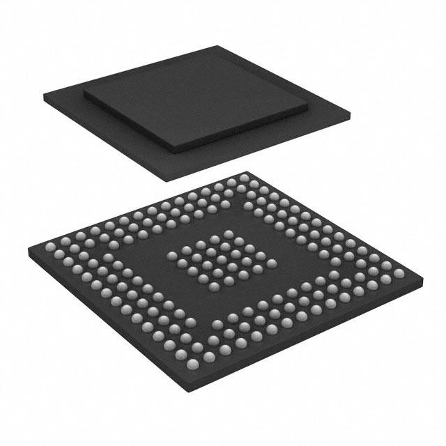
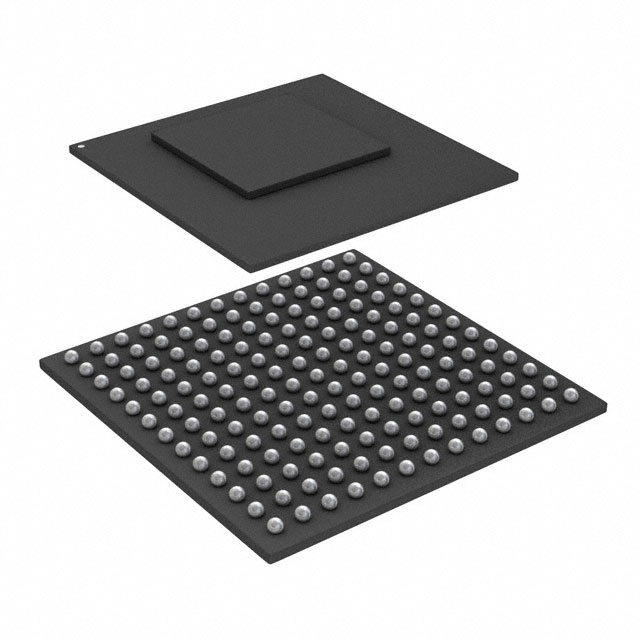
The AD9162 is a high performance, 16-bit digital-to-analog converter (DAC) that supports data rates to 6 GSPS. The DAC core is based on a quad-switch architecture coupled with a 2× interpolator filter that enables an effective DAC update rate of up to 12 GSPS in some modes. The high dynamic range and bandwidth makes these DACs ideally suited for the most demanding high speed radio frequency (RF) DAC applications.In baseband mode, wide bandwidth capability combines with high dynamic range to support DOCSIS 3.1 cable infrastructure compliance from the minimum of two carriers to full maximum spectrum of 1.794 GHz. A 2× interpolator filter (FIR85) enables theAD9161/AD9162 to be configured for lower data rates and converter clocking to reduce the overall system power and ease the filtering requirements. In Mix-Mode™operation, the AD9161/AD9162 can reconstruct RF carriers in the second and third Nyquist zones up to 7.5 GHz while still maintaining exceptional dynamic range. The output current can be programmed from 8 mA to 38.76 mA. The AD9161/AD9162 data interface consists of up to eight JESD204B serializer/deserializer (SERDES) lanes that are programmable in terms of lane speed and number of lanes to enable application flexibility.A serial peripheral interface (SPI) can configure the AD9161/AD9162 and monitor the status of all registers. The AD9161/AD9162 are offered in an 165-ball, 8.0 mm × 8.0 mm, 0.5 mm pitch, CSP_BGA package and in an 169-ball, 11 mm × 11 mm, 0.8 mm pitch, CSP_BGA package, including a leaded ball option for the AD9162.Product HighlightsHigh dynamic range and signal reconstruction bandwidth supports RF signal synthesis of up to 7.5 GHz.Up to eight lanes JESD204B SERDES interface flexible in terms of number of lanes and lane speed.Bandwidth and dynamic range to meet DOCSIS 3.1 compliance with margin.ApplicationsBroadband communications systemsDOCSIS 3.1 cable modem termination system (CMTS)/video on demand (VOD)/edge quadrature amplitude modulation (EQAM)Wireless communications infrastructureW-CDMA, LTE, LTE-A, point to pointInstrumentation, automatic test equipment (ATE)Radars and jammers
Technical Specifications
Parameters and characteristics for this part
| Specification | AD9162BBCA |
|---|---|
| Architecture | Quad-Switch |
| Data Interface | JESD204B |
| Differential Output | No |
| DNL (LSB) Tolerance | 1.7 LSB |
| INL (LSB) Tolerance | 2.7 LSB |
| Mounting Type | Surface Mount |
| Number of Bits | 16 bits |
| Number of D/A Converters | 1 count |
| Operating Temperature (Max) | 85 °C |
| Operating Temperature (Min) | -40 °C |
| Output Type | Current - Unbuffered |
| Package / Case | CSPBGA, 169-VFBGA |
| Package Length | 11 mm |
| Package Name | 169-CSPBGA |
| Package Width | 11 mm |
| Reference Type | External, Internal |
| Voltage - Supply, Analog (Range 1 Max) | 1.326 V |
| Voltage - Supply, Analog (Range 1 Min) | 1.14 V |
| Voltage - Supply, Analog (Range 2 Max) | 2.625 V |
| Voltage - Supply, Analog (Range 2 Min) | 2.375 V |
| Voltage - Supply, Digital (Max) | 1.326 V |
| Voltage - Supply, Digital (Min) | 1.14 V |
Pricing
Prices provided here are for design reference only. For realtime values and availability, please visit the distributors directly
Sign in to see pricing
Create a free account to access distributor pricing data.
CAD
3D models and CAD resources for this part
Documents
Technical documentation and resources