MAX16141AADA/VY+T
Active3.5V TO 36V IDEAL DIODE CONTROLLERS WITH VOLTAGE AND CURRENT CIRCUIT BREAKER
MAX16141AADA/VY+T
Active3.5V TO 36V IDEAL DIODE CONTROLLERS WITH VOLTAGE AND CURRENT CIRCUIT BREAKER
Description
General part information
MAX16141 Series
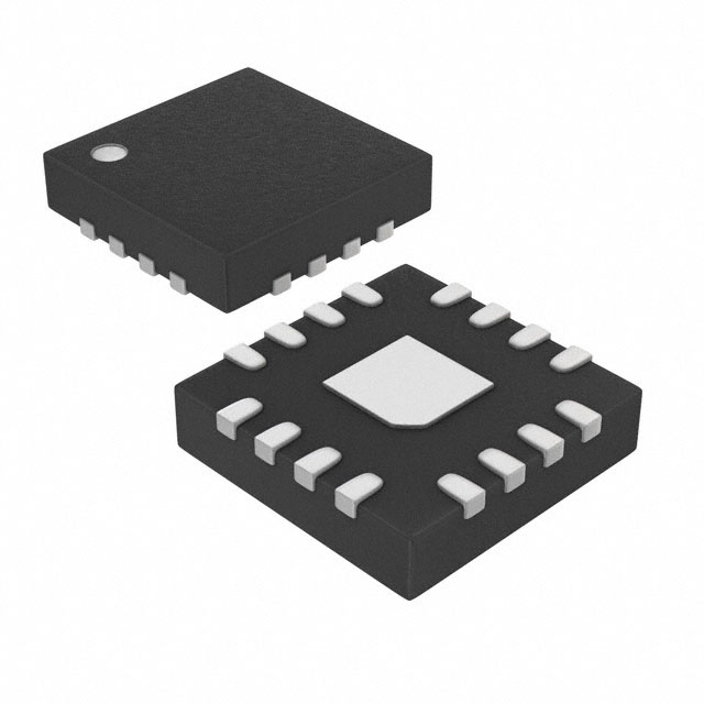
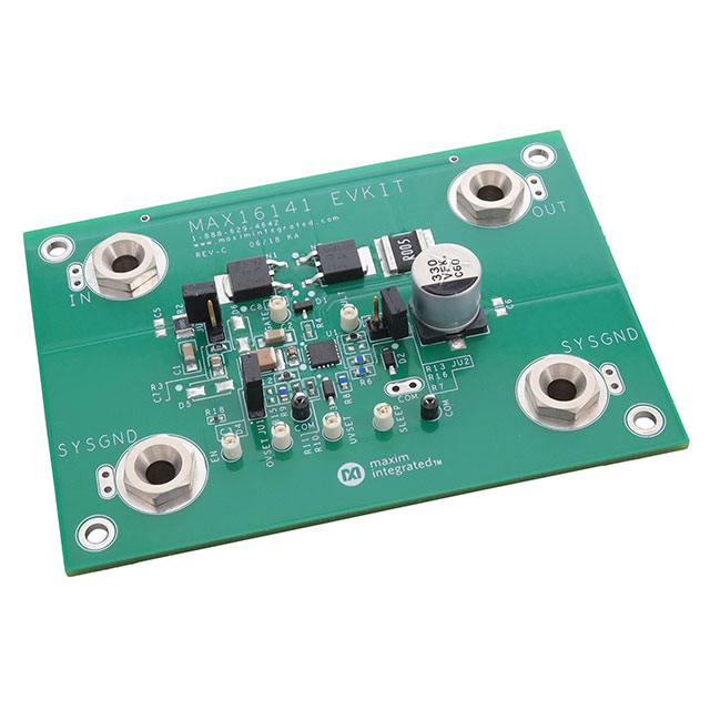
The MAX16141/MAX16141A, ideal diode controllers, provide system protection against a variety of system faults, such as reverse current, reverse voltage, overcurrent, input overvoltage/undervoltage, and overtemperature conditions. The wide operating voltage range of 3.5V to 36V, combined with 5µA (typ) of shutdown current, make the MAX16141/ MAX16141A ideal for automotive applications. An integrated charge pump drives the gate of the back-to-back external nFETs 9V above the source connection, minimizing power loss between the source and the load.A fast-acting comparator allows the MAX16141/MAX16141A to block reverse-current flow within 1µs (max) of the input falling below the output voltage. An external current-sense resistor between RS and OUT provides overload monitoring capability. Two input pins, OVSET and UVSET, provide set points to protect against input overvoltage and undervoltage events using a simple resistive-divider.During startup, the MAX16141/MAX16141A monitor the voltage drop across the external nFETs (VIN- VOUT) and the load current for overcurrent fault to ensure VOUTis greater than 0.9 x VIN. Once the startup event is complete, the MAX16141/MAX16141A are ready to protect against systems faults. During normal operation, some systems experience brownouts or short interruptions of power. To ensure smooth system recovery from these interruptions, the MAX16141/MAX16141A include a secondary power input (VCC) to keep critical circuits alive. When the main input power recovers, the MAX16141/MAX16141A enable the gate in fast mode (70µs, typ) to charge the output capacitor.Both devices feature a low-power mode that is enabled with a logic input. In low-power mode the devices allow limited current flow from source to the load. For the MAX16141, the low power mode is enabled using an active low logic input, active-low SLEEP. For the MAX16141A, the lower-power mode is activated using an active-high logic input (SLEEP).Additional features include an internal switch that isolates the monitoring from the UVSET and OVSET resistive network in shutdown mode to help minimize system power loss.The MAX16141/MAX16141A are available in a 4mm x 4mm x 0.75mm, 16-pin TQFN package and operate over the automotive temperature range of -40°C to +125°C.ApplicationsAutomotive Power SystemsNetwork/Telecom Power SystemsPoE SystemsRAID SystemsServers
Technical Specifications
Parameters and characteristics for this part
| Specification | MAX16141AADA/VY+T |
|---|---|
| Applications | Power over Ethernet (PoE) |
| Current - Supply | 2.1 mA |
| Delay Time - ON | 70 µs |
| FET Type | N-Channel |
| Grade | Automotive |
| Input Ratio | 1 |
| Internal Switch(s) | No |
| Mounting Type | Wettable Flank, Surface Mount |
| Operating Temperature (Max) | 125 °C |
| Operating Temperature (Min) | -40 °C |
| Output Ratio | 1 |
| Package / Case | 16-WQFN Exposed Pad |
| Package Length | 4 mm |
| Package Name | 16-TQFN-EP |
| Package Width | 4 mm |
| Qualification | AEC-Q100 |
| Type | N+1 ORing Controller |
| Voltage - Supply (Maximum) | 36 VDC |
| Voltage - Supply (Minimum) | 3.5 V |
Pricing
Prices provided here are for design reference only. For realtime values and availability, please visit the distributors directly
Sign in to see pricing
Create a free account to access distributor pricing data.
CAD
3D models and CAD resources for this part