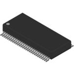
SN74CB3Q16811DGVR
Active3.3-V, 1:1 (SPST), 24-CHANNEL FET BUS SWITCH WITH PRECHARGED OUTPUTS
SN74CB3Q16811DGVR
Active3.3-V, 1:1 (SPST), 24-CHANNEL FET BUS SWITCH WITH PRECHARGED OUTPUTS
Description
General part information
SN74CB3Q16811 Series
The SN74CB3Q16811 is a high-bandwidth FET bus switch utilizing a charge pump to elevate the gate voltage of the pass transistor, providing a low and flat ON-state resistance (ron). The low and flat ON-state resistance allows for minimal propagation delay and supports rail-to-rail switching on the data input/output (I/O) ports. The device also features low data I/O capacitance to minimize capacitive loading and signal distortion on the data bus. Specifically designed to support high-bandwidth applications, the SN74CB3Q16811 provides an optimized interface solution ideally suited for broadband communications, networking, and data-intensive computing systems.
The SN74CB3Q16811 is organized as two 12-bit bus switches with separate output-enable (1OE\, 2OE\) inputs. It can be used as two 12-bit bus switches or as one 24-bit bus switch. When OE\ is low, the associated 12-bit bus switch is ON, and the A port is connected to the B port, allowing bidirectional data flow between ports. When OE is high, the associated 12-bit bus switch is OFF, and a high-impedance state exists between the A and B ports. The B port is precharged to BIASV through the equivalent of a 10-kresistor when OE\ is high, or if the device is powered down (VCC= 0 V).
During insertion (or removal) of a card into (or from) an active bus, the card’s output voltage may be close to GND. When the connector pins make contact, the card’s parasitic capacitance tries to force the bus signal to GND, creating a possible glitch on the active bus. This glitching effect can be reduced by using a bus switch with precharged bias voltage (BIASV) of the bus switch equal to the input threshold voltage level of the receivers on the active bus. This method will ensure that any glitch produced by insertion (or removal) of the card will not cross the input threshold region of the receivers on the active bus, minimizing the effects of live-insertion noise.
Technical Specifications
Parameters and characteristics for this part
| Specification | SN74CB3Q16811DGVR |
|---|---|
| Circuit | 12 x 1:1 |
| Independent Circuits | 2 |
| Mounting Type | Surface Mount |
| Operating Temperature (Max) | 85 °C |
| Operating Temperature (Min) | -40 °C |
| Package Length | 0.173 in |
| Package Name | 56-TFSOP, 56-TVSOP |
| Package Width | 4.4 mm |
| Type | Bus Switch |
| Voltage - Supply (Maximum) | 3.6 V |
| Voltage - Supply (Minimum) | 2.3 V |
| Voltage Supply Source | Single Supply |
Pricing
Prices provided here are for design reference only. For realtime values and availability, please visit the distributors directly
Sign in to see pricing
Create a free account to access distributor pricing data.
CAD
3D models and CAD resources for this part
Documents
Technical documentation and resources