


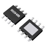
BV1LE160EFJ-CE2
ActiveRohm Semiconductor
AUTOMOTIVE IPD, 1CH LOW SIDE SWITCH WITH OUTPUT DIAGNOSTIC FUNCTION

BV1LE160EFJ-CE2
ActiveRohm Semiconductor
AUTOMOTIVE IPD, 1CH LOW SIDE SWITCH WITH OUTPUT DIAGNOSTIC FUNCTION
Description
General part information
BV1LE160EFJ-C Series
BV1LE160EFJ-C is 1ch low side switch IC for 12V automotive applications. It has built-in OCP, Dual TSD and Active Clamp function. It is equipped with output diagnostic function for TSD.
Technical Specifications
Parameters and characteristics for this part
| Specification | BV1LE160EFJ-CE2 |
|---|---|
| Current - Output (Max) | 5 A |
| Fault Protection | Over Temperature, Current Limiting (Adjustable), UVLO |
| Features | Load Discharge, Slew Rate Controlled |
| Grade | Automotive |
| Input Ratio | 1 |
| Input Type | Non-Inverting |
| Interface | Logic |
| Mounting Type | Surface Mount |
| Number of Outputs | 1 |
| Operating Temperature (Max) | 150 °C |
| Operating Temperature (Min) | -40 °C |
| Output Configuration | Low Side |
| Output Ratio | 1 |
| Output Type | N-Channel |
| Package Features | Exposed Pad |
| Package Length | 0.154 in |
| Package Name | 8-HTSOP-J, 8-SOIC |
| Package Width | 3.9 mm |
| Qualification | AEC-Q100 |
| Rds On (Typ) | 160 mOhm |
| Switch Type | General Purpose |
| Voltage - Load (Max) | 5.5 V |
| Voltage - Load (Min) | 3 V |
| Voltage - Supply (Vcc/Vdd) | Not Required |
| Voltage - Supply (Vdd/Vcc) | Not Required |
Pricing
Prices provided here are for design reference only. For realtime values and availability, please visit the distributors directly
Sign in to see pricing
Create a free account to access distributor pricing data.
CAD
3D models and CAD resources for this part
Documents
Technical documentation and resources
Datasheet
Overview of ROHM's Simulation Models(for ICs and Discrete Semiconductors)
How to Use the Two-Resistor Model
Judgment Criteria of Thermal Evaluation
Factory Information
How to Use the Thermal Resistance and Thermal Characteristics Parameters
What Is Thermal Design
HTSOP-J8 Package Information
Thermal Resistance
θ<sub>JA</sub> and Ψ<sub>JT</sub>
Design Guide and Example of Stencil for Exposed Pad
Method for Calculating Junction Temperature from Transient Thermal Resistance Data
θ<sub>JC</sub> and Ψ<sub>JT</sub>
Solder Joint Rate and Thermal Resistance of Exposed Pad
Heat Dissipation Effect of Thermal Via in Exposed Pad Type Package
Five Steps for Successful Thermal Design of IC
PCB Layout Thermal Design Guide
Impedance Characteristics of Bypass Capacitor
Basics of Thermal Resistance and Heat Dissipation