SN74LVC2G125DCT3
Active2-CH, 1.65-V TO 5.5-V BUFFERS WITH 3-STATE OUTPUTS
SN74LVC2G125DCT3
Active2-CH, 1.65-V TO 5.5-V BUFFERS WITH 3-STATE OUTPUTS
Description
General part information
74LVC2G125 Series
The SN74LVC2G125 device is a dual bus buffer gate, designed for 1.65-V to 5.5-V VCCoperation. This device features dual line drivers with 3-state outputs. The outputs are disabled when the associated output-enable (OE) input is high.
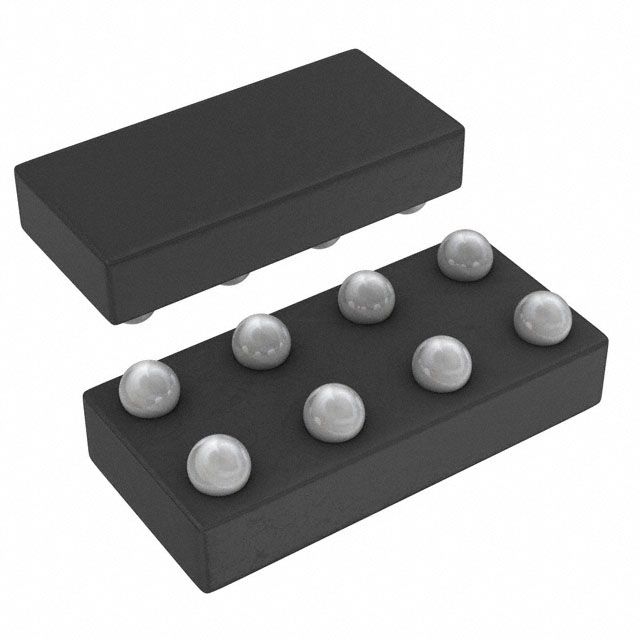
NanoFree™ package technology is a major breakthrough in IC packaging concepts, using the die as the package.
To ensure the high-impedance state during power up or power down,OEshould be tied to VCCthrough a pullup resistor; the minimum value of the resistor is determined by the current-sinking capability of the driver.
Technical Specifications
Parameters and characteristics for this part
| Specification | SN74LVC2G125DCT3 |
|---|---|
| Current - Output High | 32 mA |
| Current - Output Low | 32 mA |
| Logic Type | Buffer, Non-Inverting |
| Mounting Type | Surface Mount |
| Number of Bits per Element | 1 bits |
| Number of Elements | 2 |
| Operating Temperature (Max) | 125 °C |
| Operating Temperature (Min) | -40 °C |
| Output Type | 3-State |
| Package Length | 0.11 in |
| Package Name | 8-MSOP, 8-LSSOP, SM8 |
| Package Width | 2.8 mm |
| Voltage - Supply (Maximum) | 5.5 V |
| Voltage - Supply (Minimum) | 1.65 V |
Pricing
Prices provided here are for design reference only. For realtime values and availability, please visit the distributors directly
Sign in to see pricing
Create a free account to access distributor pricing data.
CAD
3D models and CAD resources for this part
Documents
Technical documentation and resources